
Semiconductor device and manufacturing method of the same

a semiconductor and semiconductor technology, applied in the direction of semiconductor devices, basic electric elements, electrical equipment, etc., can solve the problems of inability to commercialize transistors utilizing silicon carbide semiconductors, hollow core defects of carbide substrates, and transistors from functioning, so as to achieve high voltage and without reducing productivity

Active Publication Date: 2010-08-26
SEMICON ENERGY LAB CO LTD
View PDF12 Cites 11 Cited by
  • Summary
  • Abstract
  • Description
  • Claims
  • Application Information

AI Technical Summary

Benefits of technology

[0008]In view of the foregoing problems, an object is to provide a semiconductor device including a silicon carbide semiconductor. In addition, another object is to improve productivity of the semiconductor device including a silicon carbide semiconductor.
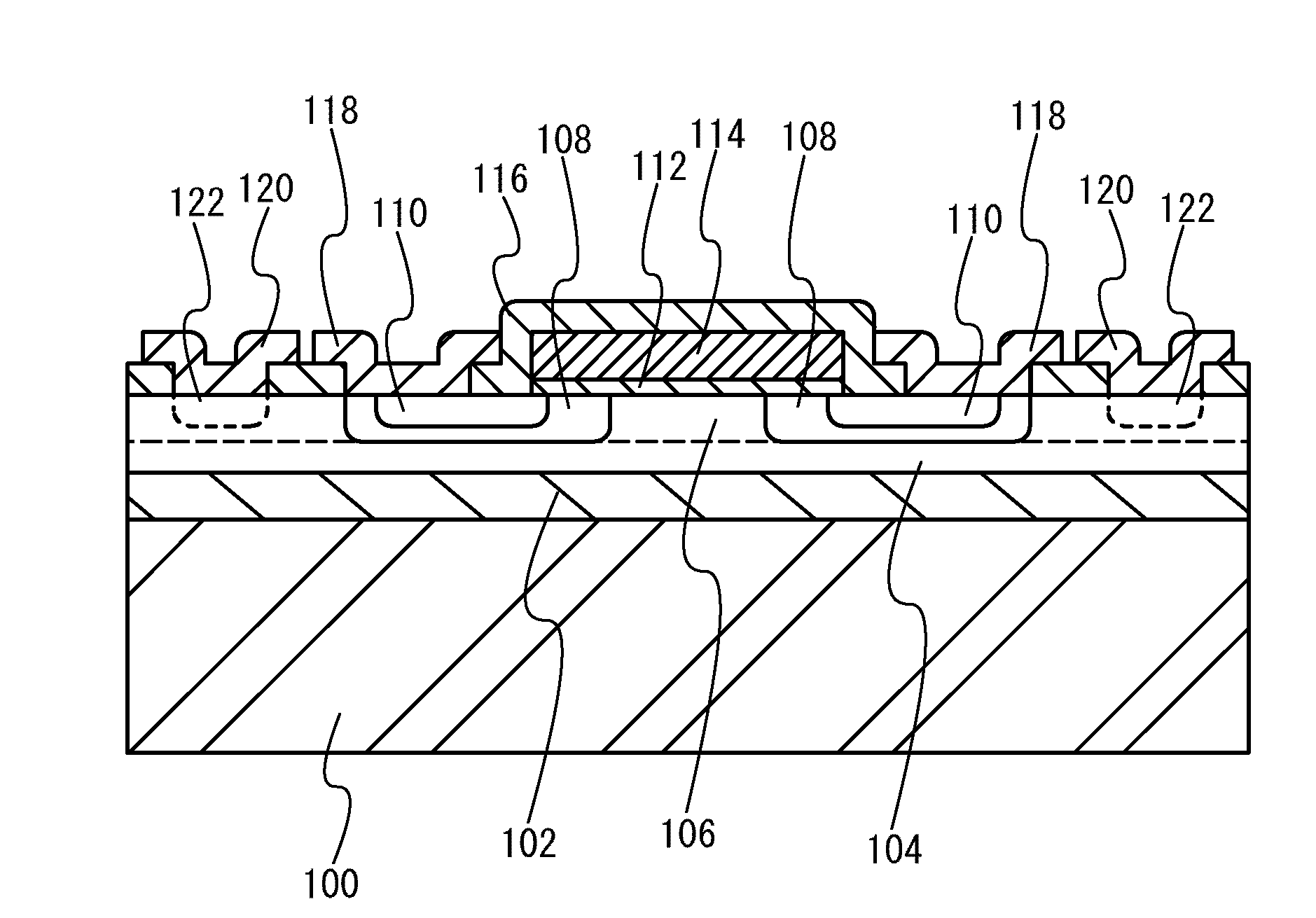
[0010]A semiconductor device according to one embodiment of the present invention includes a semiconductor layer formed on an insulating surface and at least part of the semiconductor layer is a semiconductor region having a larger energy gap than the semiconductor layer. The semiconductor region having a large energy gap is provided in a position at least overlapping with a gate electrode provided with an insulating layer interposed between the semiconductor layer and the gate electrode. A structure in which the semiconductor region having a larger energy gap than the semiconductor layer is included in a channel formation region has an effect of improving a dielectric breakdown voltage. The semiconductor layer is preferably single crystal or polycrystal, and the semiconductor region having a larger energy gap than the semiconductor layer also preferably has a crystalline structure. A preferable combination of materials is a silicon semiconductor and a carbide semiconductor, which are a material for forming the semiconductor layer and a semiconductor material having a larger energy gap than the semiconductor layer, respectively. As a carbide semiconductor, a silicon carbide is preferably used. As a silicon semiconductor, single crystal silicon is preferable, but polycrystal silicon can also be used.
[0017]A semiconductor device which withstands high voltages can be obtained by forming part or the whole of a channel formation region of a transistor from a carbide semiconductor region. By heating a semiconductor substrate or a substrate provided with a semiconductor layer in an atmosphere containing a carbide gas, a silicon carbide semiconductor layer can be formed. In this method, if the area of the semiconductor substrate or the semiconductor layer is increased, a larger apparatus may be used for heat treatment. Accordingly, a semiconductor device which includes a silicon carbide semiconductor can be manufactured without decreasing productivity.

Problems solved by technology

In spite of those advantages, commercialization of transistors utilizing a silicon carbide semiconductor has not been realized because of low quality of silicon carbide semiconductor substrates and difficulty in increasing a size of the substrates.
There is a problem in that a silicon carbide substrate has hollow-core defects called micropipes and only one micropipe in a transistor prevents the transistor from functioning.
Besides the hollow-core defects, a silicon carbide substrate has many defects such as dislocation.
Although attempts have been made to improve quality of a silicon carbide substrate, a problem of a small size of the substrate is still to be solved.
This is because crystal growth of a silicon carbide semiconductor is difficult to control.
After all, although devices including a silicon carbide semiconductor are expected to be high performance devices, their commercialization is delayed in practice due to low quality of crystals and low productivity.

Method used


Image

  • Semiconductor device and manufacturing method of the same
  • Semiconductor device and manufacturing method of the same
  • Semiconductor device and manufacturing method of the same

Examples


embodiment 1

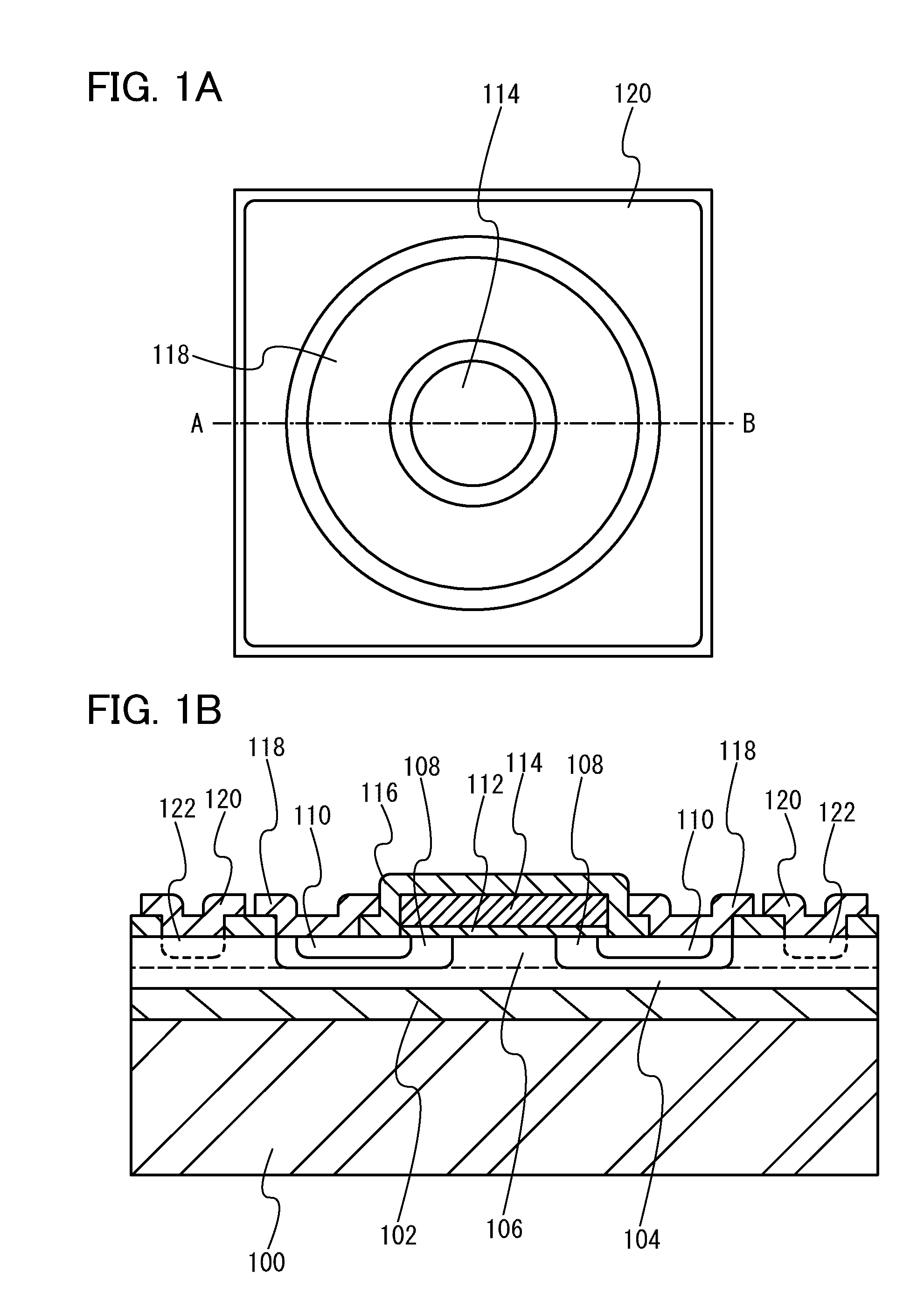
[0030]In this embodiment, an example of a semiconductor device having an SOI structure in which a semiconductor layer is provided over a support substrate with an insulating layer interposed therebetween is described. In this embodiment, an example of a structure for providing a semiconductor device including a silicon carbide semiconductor is described. FIG. 1A is a plan view of the semiconductor device and FIG. 1B is a cross-sectional view taken along dashed line A-B in the plan view.

[0031]FIG. 1A is a plan view of a semiconductor device in which a source electrode 118 is provided in the vicinity of a gate electrode 114. A drain electrode 120 is provided outside the source electrode 118. Hereinafter, a structure of a semiconductor device according to this embodiment is described with reference to FIG. 1A and a cross-sectional view in FIG. 1B.

[Support Substrate]

[0032]A substrate having a flat surface, for example, an insulating substrate, a semiconductor substrate, a metal substrat...

modification example

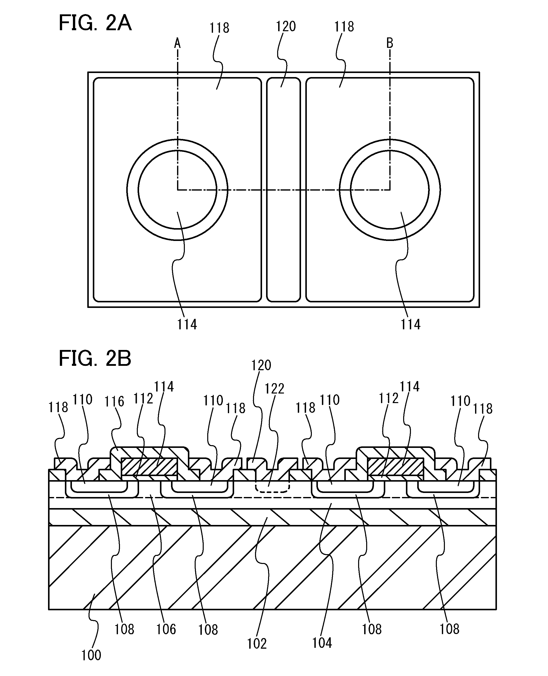
[0050]FIGS. 2A and 2B illustrate an example of a semiconductor device in which a pair of gate electrodes 114 and a pair of source electrodes 118 are provided on opposite sides of the drain electrode 120. With a structure in which two channel formation regions are provided in the support substrate 100 and the drain electrode 120 is sandwiched by the two source electrodes 118, a device can be downsized while allowing a large amount of current to flow. Such a semiconductor device is suitable for applications with high rated current.

[Operation of Semiconductor Device]

[0051]In the case where the semiconductor layer 104 has an n-type conductivity, the first impurity region 108 has a p-type conductivity, and the second impurity region 110 has an n-type conductivity, an npn junction is formed between the source electrode 118 and the drain electrode 120. Accordingly, when bias is not applied to the gate electrode, only a small amount of current flows.

[0052]When positive bias is applied to th...

embodiment 2

[0055]In this embodiment, an example of a method of manufacturing the semiconductor device described in Embodiment 1 is described with reference to FIGS. 3A and 3B, FIGS. 4A and 4B, and FIGS. 5A and 5B. An object of this embodiment is to provide a semiconductor device including a silicon carbide semiconductor. In addition, another object of this embodiment is to improve productivity of the semiconductor device including a silicon carbide semiconductor.

[Manufacture or Preparation of Support Substrate (see FIG. 3A)]

[0056]The semiconductor layer 104 is formed over the support substrate 100 with the insulating layer 102 interposed therebetween. This is a so-called SOI structure in which a semiconductor layer is provided over an insulating surface. Therefore, SOI substrates which are commercially available such as a bonded SOI substrate, a SIMOX (separation by implanted oxygen) substrate, or the like can be employed. A material of the semiconductor layer 104 is preferably single crystal ...


PUM


Abstract

At least part of a semiconductor layer or a semiconductor substrate includes a semiconductor region having a large energy gap. The semiconductor region having a large energy gap is preferably formed from silicon carbide and is provided in a position at least overlapping with a gate electrode provided with an insulating layer between the semiconductor region and the gate electrode. By making a structure in which the semiconductor region is included in a channel formation region, a dielectric breakdown voltage is improved.

Description

BACKGROUND OF THE INVENTION[0001]1. Field of the Invention[0002]One mode of this disclosed invention relates to semiconductor devices and a manufacturing method thereof. Further, one mode of the present invention relates to semiconductor devices which control a relatively large amount of electrical power.[0003]2. Description of the Related Art[0004]An energy gap of a silicon carbide semiconductor (4H—SiC) is 3.02 eV, which is about three times that of a silicon semiconductor, 1.12 eV. A dielectric breakdown electric field of a silicon semiconductor is 0.3 MV / cm while a dielectric breakdown electric field of a silicon carbide semiconductor is 3.5 MV / cm, which is more than ten times as high as that of a silicon semiconductor. Therefore, the use of a silicon carbide semiconductor for electrical devices typified by inverters and converters is expected.[0005]In spite of those advantages, commercialization of transistors utilizing a silicon carbide semiconductor has not been realized beca...

Claims


Application Information

Patent Timeline
IPC IPC(8): H01L29/24H01L21/336
CPCH01L21/76254H01L29/0696H01L29/0882H01L29/1608H01L29/165H01L29/7395H01L29/7802H01L29/7809H01L29/7824H01L29/66068
Inventor YAMAZAKI, SHUNPEIARAI, YASUYUKI
Owner SEMICON ENERGY LAB CO LTD
Learn More