Image pickup apparatus

Active Publication Date: 2010-09-09
RENESAS ELECTRONICS CORP
View PDF5 Cites 89 Cited by
  • Summary
  • Abstract
  • Description
  • Claims
  • Application Information

AI Technical Summary

Benefits of technology

[0014]According to the invention, the following processing is carried out when electric charges generated at each photoelectric conversion element are read: a coupling transistor is switched on or off according to light exposure. This makes it possible to vary the capacity of each charge storage portion and

Problems solved by technology

In these technologies, however, the percentage of the area occupied by a photodiode in a pixel is reduced as compared with conventional cases because of the addition of the capacitive element and it is suspected to be difficult to maintain high picture

Method used


Image

  • Image pickup apparatus
  • Image pickup apparatus
  • Image pickup apparatus

Examples


Example

First Embodiment

Configuration of Image Pickup Apparatus 1

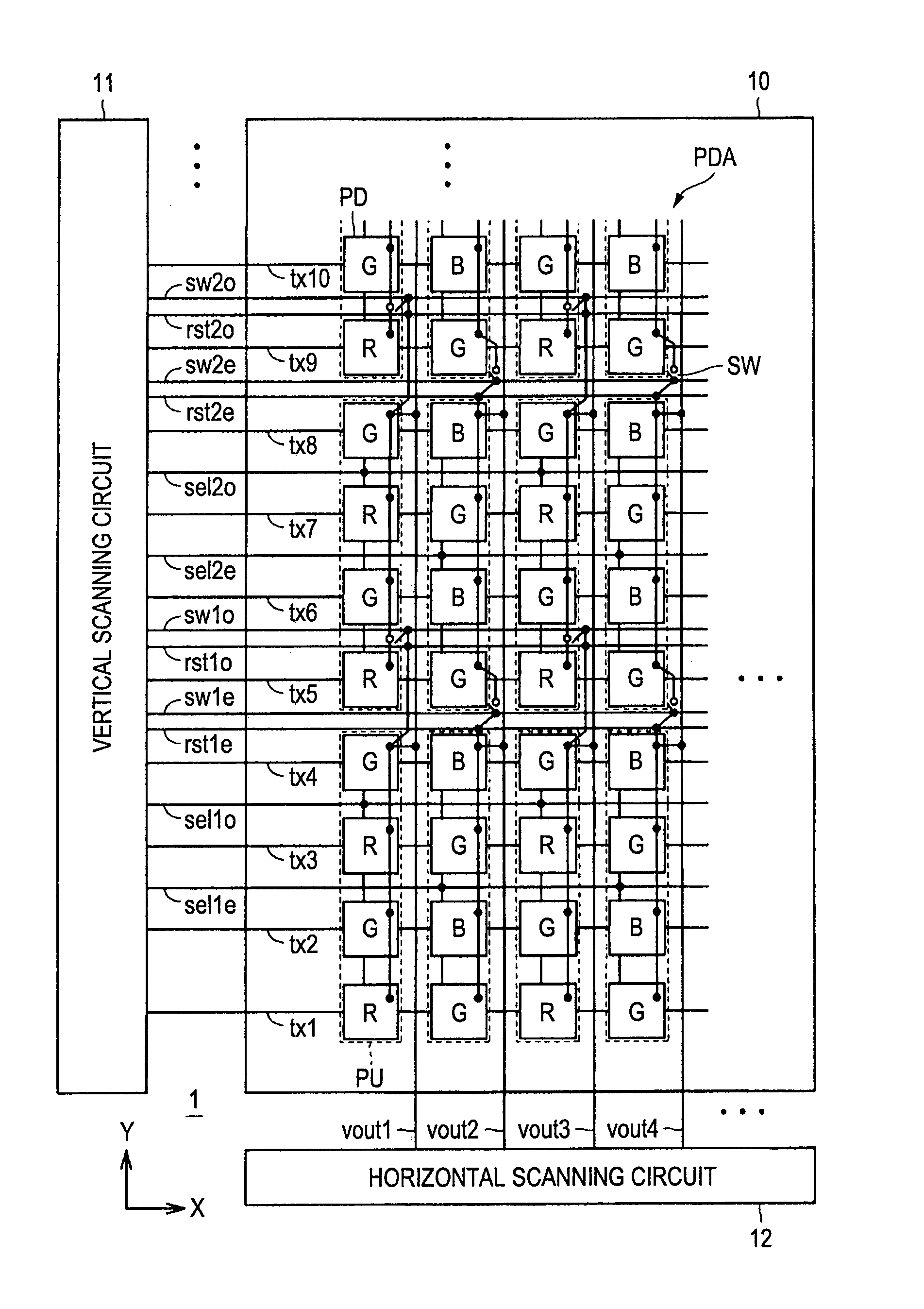
[0025]FIG. 1 is a block diagram illustrating the configuration of an image pickup apparatus 1 in a first embodiment of the invention.

[0026]As illustrated in FIG. 1, the image pickup apparatus 1 includes a pixel array portion 10, a vertical scanning circuit 11, a horizontal scanning circuit 12, multiple control signal lines tx, rst, sel, sw, and multiple output signal lines vout.

[0027]The pixel array portion 10 includes a photodiode array PDA (photoelectric conversion element array) comprised of multiple photodiodes PD (photoelectric conversion elements) arranged in a matrix pattern. In FIG. 1, a photodiode array PDA of 10 rows and four columns is shown for the sake of simplicity. Specifically, photodiodes PD in the first column to the fourth column are shown from left to right in FIG. 1 and photodiodes PD in the first row to the 10th row are shown from bottom up in FIG. 1. The left and right direction in FIG. 1 will be designa...

Example

Second Embodiment

[0129]FIG. 8 is a plan view schematically illustrating the layout of a pixel array portion 10A. The layout of the pixel array portion 10A in FIG. 8 is a modification to the layout of the pixel array portion 10 in the first embodiment illustrated in FIG. 7. FIG. 8 depicts photodiodes PD in the first and second columns (C1, C2) and in the fifth row to the eighth row (R5 to R8) of the photodiode array PDA. The photodiodes PD are arranged over a semiconductor substrate at equal intervals both in the column direction and in the row direction. In the following description, the same or equivalent parts as in FIG. 7 will be marked with the same reference marks and the description thereof may not be repeated.

[0130]In the pixel array portion 10A, four photodiodes PD in each column of the photodiode array PDA comprise a group and each group corresponds to a pixel unit PU. In case of the example in FIG. 8, specifically, the pixel unit PU2a includes the photodiodes PD5a, PD6a, P...


PUM


Abstract

An image pickup apparatus that makes it possible to achieve both high picture quality and a wide dynamic range is provided. Each pixel unit included in the image pickup apparatus includes: four photodiodes; four transfer transistors; a charge storage portion (four floating diffusions) for storing electric charges generated at the photodiodes; an amplification transistor; a select transistor; and a reset transistor. The image pickup apparatus further includes multiple coupling transistors. Each coupling transistor couples together the charge storage portions of two pixel units of the pixel units. A scanning circuit switches on or off the coupling transistors according to read mode.

Description

CROSS-REFERENCE TO RELATED APPLICATIONS[0001]The disclosure of Japanese Patent Application No. 2009-53724 filed on Mar. 6, 2009 including the specification, drawings and abstract is incorporated herein by reference in its entirety.BACKGROUND OF THE INVENTION[0002]The present invention relates to an image pickup apparatus having a photoelectric conversion function.[0003]Image sensors of CCD (Charge Coupled Device), CMOS (Complementary Metal-Oxide Semiconductor), and the like are required that their dynamic range should be widened with high sensitivity and a high S / N (Signal-to-Noise) ratio maintained. As image pickup apparatuses whose dynamic range can be widened, for example, the following technologies are known.[0004]In the technology disclosed in Japanese Unexamined Patent Publication No. 2006-217410 (Patent Document 1), each pixel of an image pickup apparatus includes the following: a photodiode, a transfer transistor, a floating diffusion (floating area), an overflow gate, a sto...

Claims


Application Information

Patent Timeline
IPC IPC(8): H04N5/335H04N5/355H04N5/369H04N5/374H04N5/376
CPCH01L27/14609H04N5/347H04N5/3559H01L27/14641H04N5/37457H04N5/335H04N5/37452H01L27/14603H01L27/14645H04N25/46H04N25/59H04N25/778H04N25/771H04N25/00H04N25/75
Inventor SUZUKI, ZENZODOSAKA, KATSUMI
Owner RENESAS ELECTRONICS CORP
Why Eureka
Try Eureka