High electron mobility field effect transistor (HEMT) device

a field effect transistor and high electron mobility technology, applied in the field of field effect transistors, can solve problems such as insufficient and satisfactorily solved problems, affecting system reliability, and system failure to function and perform properly, and achieve the effects of improving heat dissipation mechanisms, high electron mobility transistors, and improving hemt efficiency

Inactive Publication Date: 2010-09-16
CHANG GUNG UNIVERSITY
View PDF5 Cites 11 Cited by
  • Summary
  • Abstract
  • Description
  • Claims
  • Application Information

AI Technical Summary

Benefits of technology

[0008]A major objective of the present invention is to provide a High Electron Mobility Transistor (HEMT) device, so as to overcome the shortcomings of the prior art. In this respect, the present invention is realized by means of flip-chips, wherein, the HEMT's are mounted onto a sub-mount, so that HEMT may have a better heat dissipation mechanism, thus increasing the efficiency of HEMT and prolong its service life span.
[0009]Therefore, in order to achieve the above-mentioned objective, the HEMT disclosed by the present invention comprises: an input terminal, an output terminal, and a plurality of flip-chip type HEMT elements. The plurality of flip-chip type HEMT elements can each connected to the input terminal and the output terminal in parallel, or they can be connected with each other in series and in parallel in combination, and then this combined structure is connected to the input terminal and output terminal to form a tree-shaped structure, such that the distances between each of the flip-chip type HEMT elements, from each element to the input terminal, and from each element to the output terminal are equal. Therefore, in this configuration, the power consumed by each of th

Problems solved by technology

In general, the operation temperature of electronic elements will greatly affect the reliability of a system.
Thus, when the operation temperature exceeds a certain allowable limit, its physical properties tend to change, thus making the system to function and perform out of order.
When HEMT

Method used


Image

  • High electron mobility field effect transistor (HEMT) device
  • High electron mobility field effect transistor (HEMT) device
  • High electron mobility field effect transistor (HEMT) device

Examples


Embodiment Construction

[0022]The purpose, construction, features, functions and advantages of the present invention can be appreciated and understood more thoroughly through the following detailed description with reference to the attached drawings.

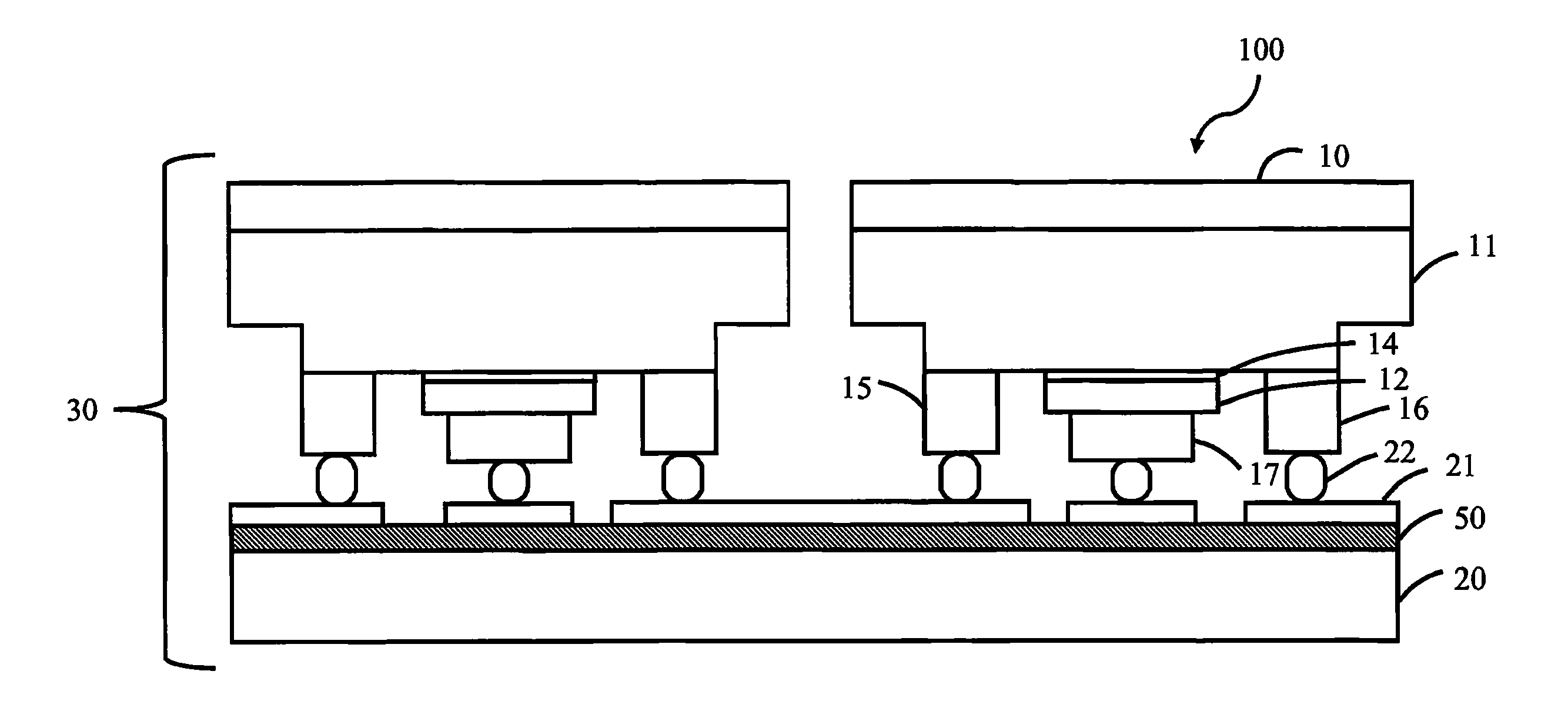
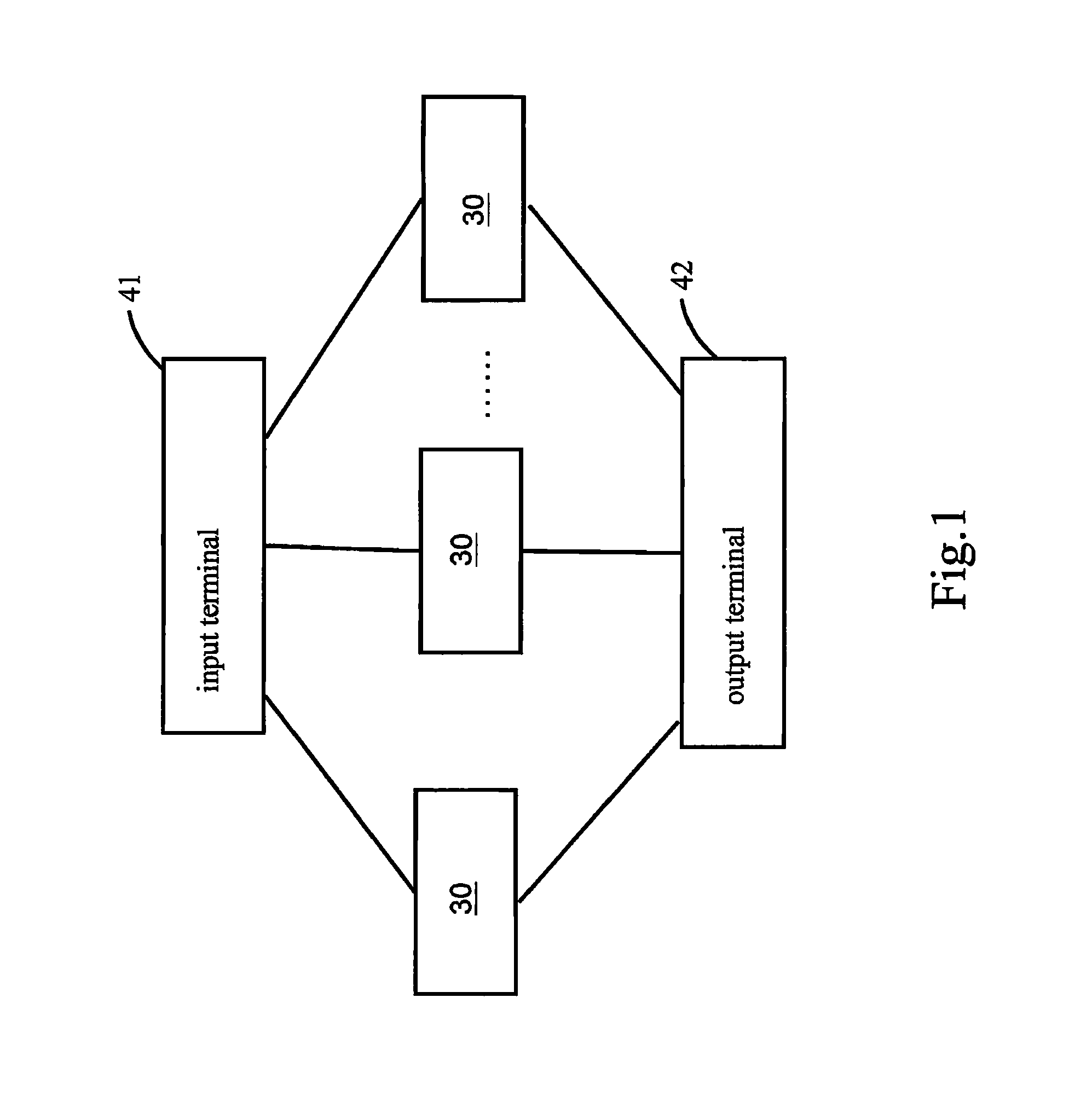
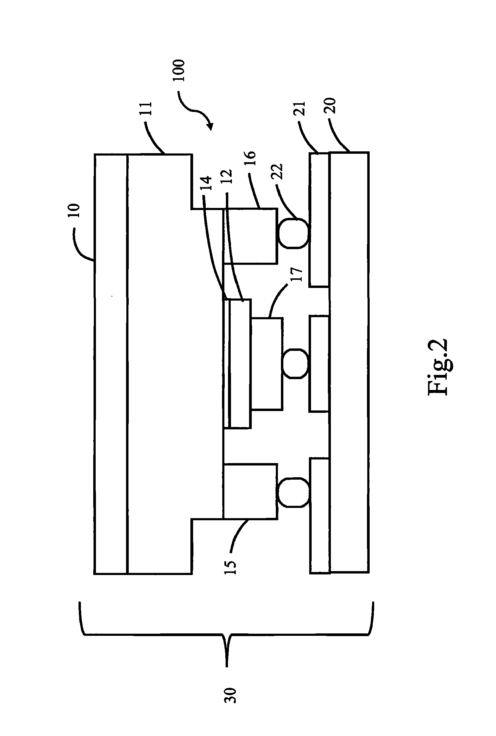
[0023]Refer to FIG. 1 for a schematic diagram of a High Electron Mobility Transistor (HEMT) device according to a first embodiment of the present invention. As shown in FIG. 1, a High Electron Mobility Transistor (HEMT) Device includes an input terminal 41, an output terminal 42, and a plurality of flip-chip type High Electron Mobility Transistor (HEMT) element 30; and each of a plurality of flip-chip type High Electron Mobility Transistor (HEMT) element 30 is connected to the input terminal 41 and output terminal 42 in parallel. In other words, each of the flip-chip type HEMT element 30 is connected to the input terminal 41 and output terminal 42 respectively. Meanwhile, the distance from each of the flip-chip type HEMT element 30 to the input terminal 41 is d...


PUM


Abstract

A High Electron Mobility Transistor (HEMT) device, which is formed by connecting a plurality of low power flip-chip type High Electron Mobility Transistor (HEMT) elements in parallel, or connected them in parallel and in series in combination into a tree-shaped structure, and then connecting said structure to an input terminal and an output terminal. Distances between each of the flip-chip type HEMT elements, from each element to said input terminal, and from each element to said output terminal are designed to be equal, such that powers consumed by each of the flip-chip type HEMT elements are equal, currents flowing through are evenly distributed, and heat generated is liable to be dissipated. A spike leakage protection layer, such as zinc-oxide (ZnO) amorphous layer or poly-crystal layer, is further included, hereby further enhancing the efficiency of said flip-chip type HEMT element and prolonging its service life.

Description

BACKGROUND OF THE INVENTION[0001]1. Field of the Invention[0002]The present invention relates to a field effect transistor (FET) device, applicable in high frequency and high power microwave range, and in particular to a high electron mobility field effect transistor (HEMT) device, wherein, a plurality of low-power flip-chip type HEMT's are connected in parallel, or are connected to form a tree-shaped structure through a combination of series connections and parallel connections, so as to dissipate its heat generated, increase its efficiency, and prolong its service life span.[0003]2. The Prior Arts[0004]In recent years, the high electron mobility field effect transistor (HEMT) device is a hot topic and widely popular in the high frequency and high power microwave sphere. Since gallium nitride (GaN) material has the property of high chemical inertness, good heat stability, and strong bonding force, as such, it demonstrates superior heat resistant and corrosion resistant capability i...

Claims


Application Information

Patent Timeline
IPC IPC(8): H01L29/778
CPCH01L25/072H01L29/2003H01L2224/81192H01L2224/16225H01L29/7786H01L2224/0554H01L2224/05568H01L2224/05573H01L2224/056H01L2924/00014H01L2924/12032H01L2924/00H01L2224/05599H01L2224/0555H01L2224/0556
Inventor CHANG, LIANN-BECHIU, HSIEN-CHINLEE, YUN-LINLIN, CHAO-WEIDAS, ATANU
Owner CHANG GUNG UNIVERSITY
Why Eureka
Try Eureka