Touch pad for multiple sensing

a technology touch pads, applied in the field of touch pads, can solve the problems of more complex control circuit chips, more complex manufacturing processes of capacitive touch pads, and high cost of resistance-sensitive touch pads

Inactive Publication Date: 2010-09-16
MEMSOR CORP
View PDF2 Cites 37 Cited by
  • Summary
  • Abstract
  • Description
  • Claims
  • Application Information

AI Technical Summary

Benefits of technology

[0021]In order to overcome the limitations of the prior art, an object of the present invention is to provide a touch pad for multiple sensing having the advantages of a capacitive and a resistance-sensitive touch pad at the same time with a two-layer structure. The touch pad for multiple sensing comprises an upper conductive layer and a lower conductive layer. The upper conductive layer has a plurality of upper sensor members and a plurality of electrically coupled upper joint members. The plurality of upper sensor members are disposed on middle of one surface of the upper conductive layer and the plurality of upper joint members are disposed on border of one surface of the upper conductive layer. The lower conductive layer has a plurality of lower sensor members and a plurality of electrically coupled lower joint members. The plurality of lower sensor members are disposed on middle of one surface of the lower conductive layer and the plurality of lower joint members are disposed on border of one surface of the lower conductive layer. In addition, the lower sensor members are disposed against the upper sensor members in a certain distance.

Problems solved by technology

In addition, resistance-sensitive touch pads are cost competitive and are mostly used in consumer electronic products such as cell phones, personal digital assistants (PDAs), and global position systems (GPSs).
On the other hand, the manufacturing process of capacitive touch pads are more complex and the control circuits chip are more complicated than the resistance-sensitive touch pad, capacitive touch pads are mostly used in the premium electronic devices such as notebook computers and automatic teller machines (ATMs).
Sound wave and the optical touch pads are mostly applied in premium electronic products with large dimensions because the technology and manufacturing processes are not ready at a massive production scale.
However, the operation on a resistance-sensitive touch pad involves pressing and clicking which lead to strain fatigue of the upper and the lower conductive films 15, 17 and the top plate 14.
Therefore, a resistance-sensitive touch pad has a limited life and it is not suited for applications used on regular basis or public applications used frequently.
That means, when the tip size of object is thicker (for example: a bigger finger or a blunt object), the position of the touch point can not be precisely measured.
Moreover, the distance calculated by a resistance-sensitive touch pad is deviated due to that surface resistance on conductive films is subject to temperature.
Resistance-sensitive touch pads are also not recommended to operate in an environment under high temperature or significant temperature changes for the temperature sensitivity of conductive film.
However, when a conductive film has undesirable uniformity, worn out due to repetitive operations, or placed under higher temperature, the distance attained by succeeding calculation of signal processing modules then is deviated.
Moreover, the prior art resistance-sensitive touch pad is not configured to receive pressing signals from multi-contact points.
There are many limitations existed in the application of prior art resistance-sensitive touch pads.
However it is easily affected by interference of surrounding electromagnetic waves, human physical condition (fingers), and ambient humidity.
Therefore the capacitive touch pad is not suited for applications under conditions such as high humidity, contacting with fingers in gloves or wet fingers, as well as configured, equipped or used in devices generating electromagnetic waves, specifically electromagnetic wave with frequency in the capacitance sensing range of the touch pad.
However, the resistance-sensitive touch pad and the capacitive touch pad alone no longer meet the market demands as designs of portable devices are getting smaller and with extra adding functions.
For example, resistance-sensitive touch pads are only applicable to single point touch in the prior art and not applicable to multi-finger touch gesture.
In addition, resistance-sensitive touch pads are only suited for private application used infrequently, devices usually have short life, also coordinates offset with temperature.
Capacitive touch pads deliver multi-finger gesture sensing, but do not have sharp sensing resolution as resistance-sensitive touch pads operated by a pencil-shaped object.
Also, capacitive touch pads are easily affected by human body condition, ambient humidity, and surrounding electromagnetic wave intensity.
Consequently, the multi-function touch pads become too bulky and heavy to use in portable devices.
Moreover, the stacking structure of a capacitive type pad on a resistance-sensitive type pad generates light transmittance which is far below expected light transmittance.
The resulted light transmittance is much lower than light transmittance of devices available on the shelf and is uncompetitive in the market.
When users perform writing and plotting function with the resistance-sensitive touch pad operation, operation may become slow, crashed, or intermittent.
There are challenges in manufacturing process and cost control of the production for such touch pad stacking a capacitive type pad and a resistance-sensitive pad.
Firstly, by stacking pads of two types, the overall manufacturing process and the cost are not saved.
In fact, the process demands extra steps to stack two touch pads.
Thirdly, there is one transmitting cable added which requires rewiring to connect the cable to the succeeding signal processing modules and requires extra cost due the assembly process and wiring work of the cable added.

Method used


Image

  • Touch pad for multiple sensing
  • Touch pad for multiple sensing
  • Touch pad for multiple sensing

Examples


first embodiment

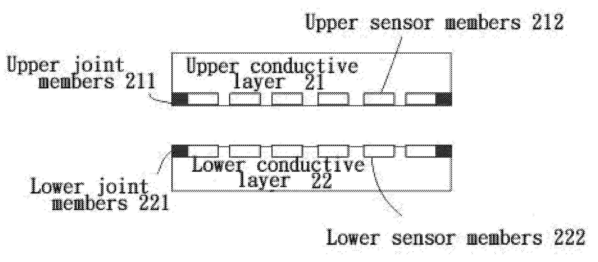
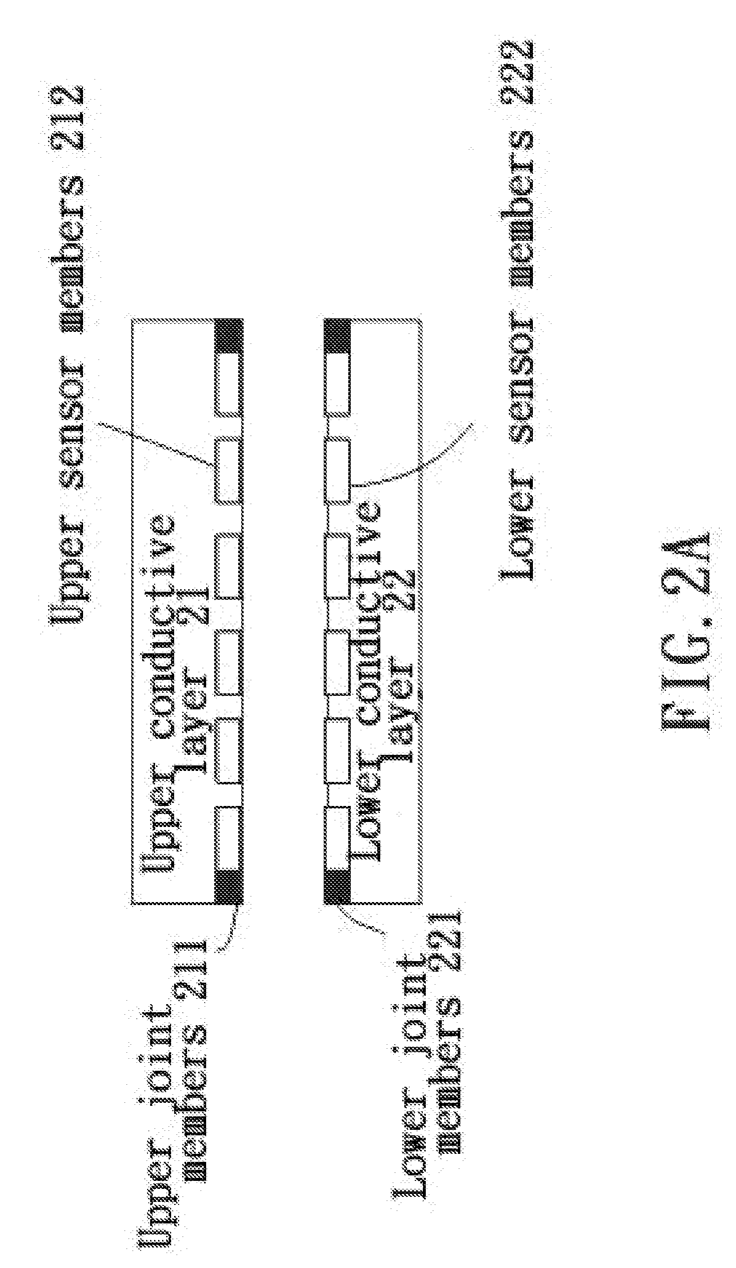
[0039]the present invention is shown in FIG. 2A. The embodiment comprises: an upper conductive layer 21 and a lower conductive layer 22. The surface of the upper conductive layer 21 includes a plurality of upper sensor members 212 disposed in the middle and a plurality of upper joint members 211 disposed on the edge. The surface of the lower conductive layer 22 also includes a plurality of lower sensor members 222 disposed in the middle and a plurality of lower joint members 221 disposed on the edge. The upper conductive layer 21 is disposed relative to the lower conductive layer 22 by a distance, such that the surfaces of the upper sensor members 212 and the lower sensor members 222 are disposed opposite each other. The distance is relative to the areas, thicknesses and material structures of the upper sensor members and the lower sensor members, as well as dielectric of the space between the upper conductive layer and the lower conductive layer.

[0040]The upper conductive layer 21 ...

second embodiment

[0048]the present invention is as shown in FIG. 2B, which comprises an upper conductive layer 21, a conducting layer 23 and a lower conductive layer 22. The surface of the upper conductive layer 21 includes a plurality of upper sensor members 21 in the middle and a plurality of upper joint members 211 on the edge. The surface of the conducting layer 23 includes a plurality of conductive bridges 231 in the middle, and the conductive bridges are disposed on the surface between any two of the upper sensor members 212 to enable the electrical conduction between any two of the upper sensor members 212. The surface of the lower conductive layer 22 has a conductive film 223 and a plurality of lower joint members 221. The upper conductive members 21 are disposed relative to the lower conductive members 22 at a distance, such that the surfaces of the upper sensor members 212 and the lower sensor members 222 and the conductive bridges 231 are disposed oppositely. The distance is relative to t...


PUM


Abstract

A touch pad for multiple sensing configured to receive touch and pressed-pressure made from at least one finger, conductor or object, comprising an upper conductive layer and a lower conductive layer underneath the upper conductive layer. The upper conductive layer has a plurality of upper sensor members and a plurality of upper joint members. The lower conductive layer has a plurality of lower sensor members and a plurality of lower joint members. The distance-related capacitance on upper sensor members and lower sensor members are detected through the electrically coupled upper joint members and the electrically coupled lower joint members respectively. Besides, an overlapped portion of the upper sensor members and the lower sensor members are electrically conducted by the pressed-pressure. Meanwhile, at least one electrical signal is generated from voltage difference between the upper joint members or between the lower joint members, which the strength of electrical signal is related to the distance of pressed-pressure from the upper joint members or from the lower joint members.

Description

BACKGROUND OF THE INVENTION[0001]1. Field of the Invention[0002]The present invention is related to a touch pad, particularly to a touch pad having functions of the resistance-sensitive type and the capacitive type touch pad in a simplified structure.[0003]2. Brief Description of the Related Art[0004]With the rapid development of portable interactive electronic products, touch pads have become a common device required in an electronic product. In order to meet the market demand to integrate touch pads in the product designs, not only the quality and performance of touch pads are improved, also the cost is lowered and the yield rate is raised. Touch pads are configured according to various design mechanisms, which can be categorized into four types. These types are resistance-sensitive, the capacitive, the acoustic wave, and the optical touch pads. Each design mechanism gives the touch pad different manufacturing processes, functions, instructions, and applications with individual ad...

Claims


Application Information

Patent Timeline
Patent Type & Authority Applications(United States)
IPC IPC(8): G06F3/041
CPCG06F3/044G06F2203/04106G06F3/045G06F3/0445
Inventor LIN, JAO-CHINGCHU, LINABELCHANG, CHANG-SHENG
Owner MEMSOR CORP
Why Eureka
Try Eureka