Optical Control Device

a control device and optical waveguide technology, applied in the direction of optics, non-linear optics, instruments, etc., can solve the problems of affecting the speed matching between a light wave propagating through the optical waveguide and a modulated signal, and the efficiency of the electro-optical effect, so as to reduce the cost of a driving device, reduce the driving voltage, and increase the confinement efficiency of a light wave

Active Publication Date: 2010-09-16
SUMITOMO OSAKA CEMENT CO LTD
View PDF14 Cites 30 Cited by
  • Summary
  • Abstract
  • Description
  • Claims
  • Application Information

AI Technical Summary

Benefits of technology

[0031]By the invention related to claim 1, since an optical control device including a thin plate which has an electro-optical effect and has, a thickness of 10 μm or less, an optical waveguide formed in the thin plate, and control electrodes for controlling light passing through the optical waveguide is configured such that the control electrodes are configured to include a first electrode and a second electrode disposed to interpose the thin plate therebetween, the first electrode has a coplanar type electrode including at least a signal electrode and a ground electrode, and the second electrode has at least a ground electrode and is configured to apply an electric field to the optical waveguide in cooperation with the signal electrode of the first electrode, speed matching between a microwave and a light wave or impedance matching of microwaves can be realized and accordingly, it is possible to provide an optical control device which can operate in high speed. In addition, since a driving voltage can be reduced, high-speed driving using an existing cheap driving device becomes possible. As a result, the cost related to a driving device can also be reduced.
[0032]By the invention related to claim 2, since the optical waveguide is a ridge type optical waveguide, the confinement efficiency of a light wave is increased and it becomes possible to concentrate an electric field, which is formed by control electrodes, on the optical waveguide. Accordingly, an optical control device with a lower driving voltage can be realized.
[0033]By the invention related to claim 3, since a buffer layer is formed between the thin plate and the firs...

Problems solved by technology

In the case of the coplanar type control electrode, however, an external electric field does not act efficiently in the direction (vertical direction in the case of the Z-cut type LiNbO3 substrate shown in FIG. 1A) where the efficiency of the electro-optical effect of the substrate 1 is high.
However, in the electrode structure shown in FIG. 10, the refractive index of a microwave increases and accordingly, speed matching between a light wave propagating through the optical waveguide and a microwave which is a modulated signal becomes difficult.
In addition, since impedance decreases conversely, there is a disadvantage that impedance matching with a signal line of ...

Method used


Image

  • Optical Control Device
  • Optical Control Device
  • Optical Control Device

Examples


embodiments

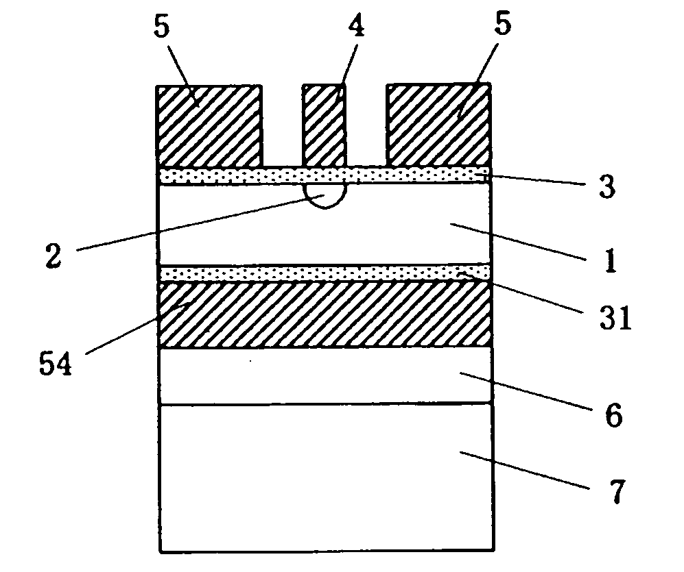
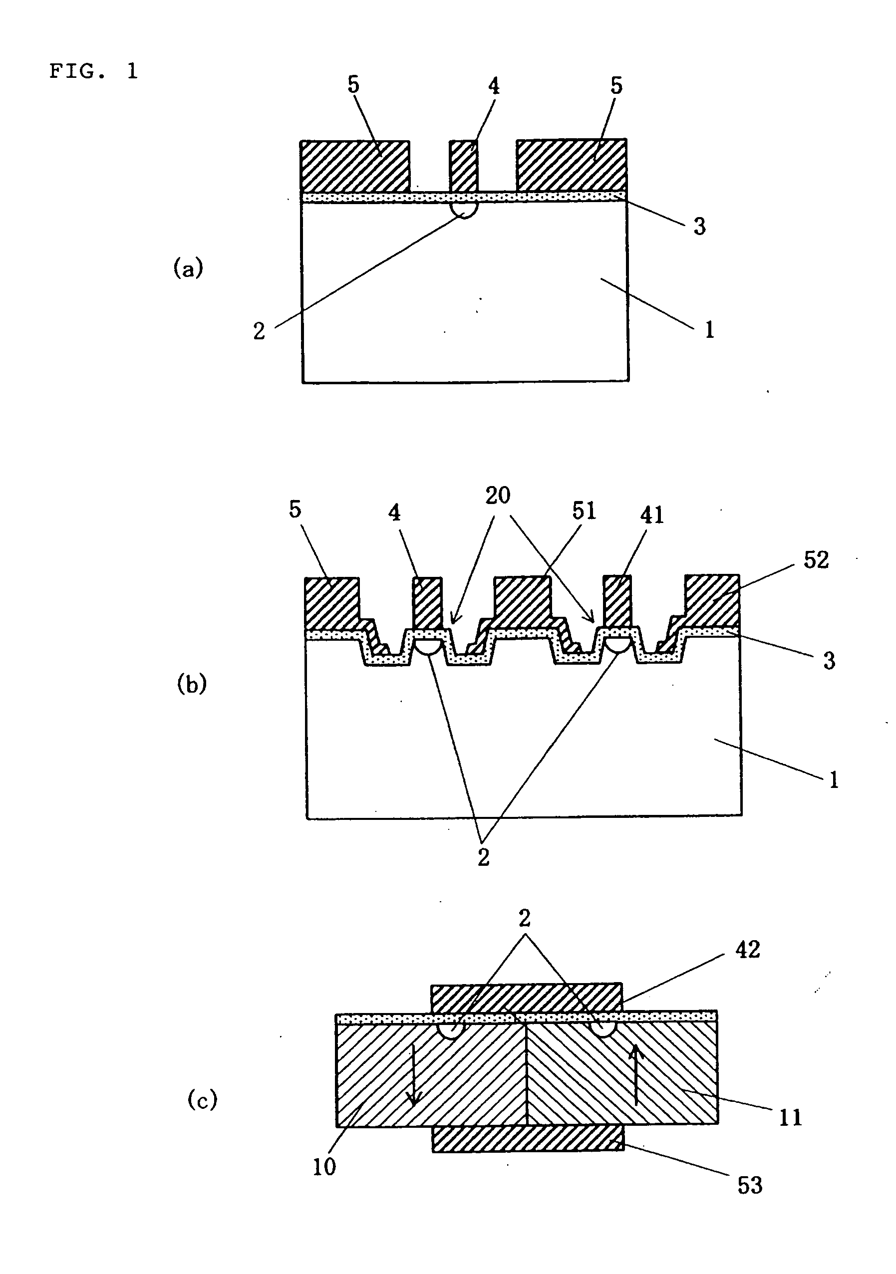
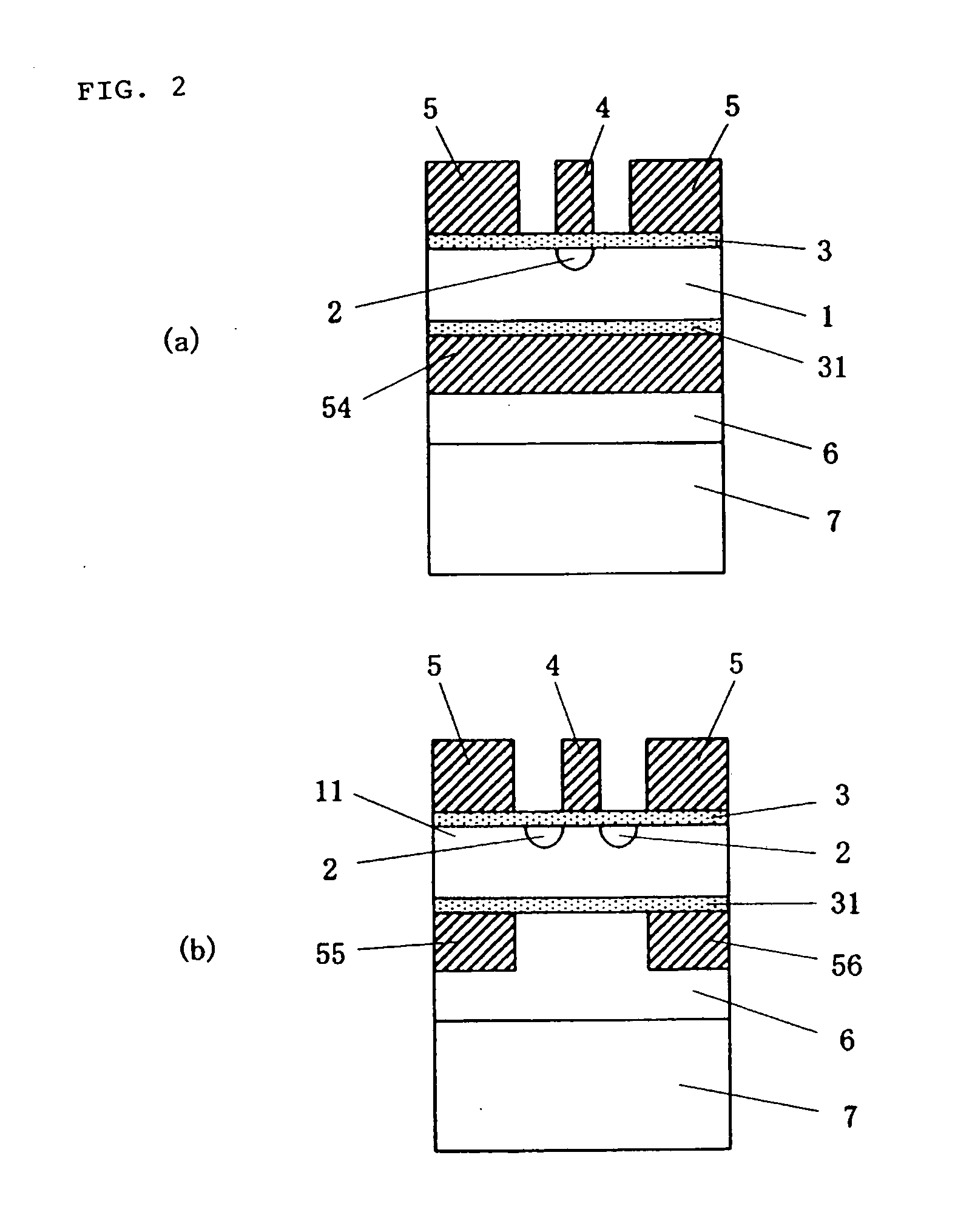
[0143]In order to see the basic characteristics of the optical control device of the present invention, a change in a driving voltage value (V·cm) in a substrate thickness range of 2 to 10 μm was calculated in an embodiment in which a coplanar electrode is provided on a top surface side of a substrate and a ground electrode is disposed on a bottom surface side as shown in FIG. 3A, a first known technique example in which only a coplanar electrode is disposed on the substrate surface as shown in FIG. 1A, and a second known technique example in which a substrate is interposed between control electrodes on top and bottom surface sides of the substrate as shown in FIG. 1C. In the embodiment, it was assumed that height of the signal electrode 4 / thickness of the substrate 1 was 1.25, width of the signal electrode 4 / thickness of the substrate 1 was 1.5, gap between the signal electrode 4 and the ground electrode 5 / thickness of the substrate 1 was 3, height of the ridge portion 20 / thickness...


PUM


Abstract

It is an object to provide an optical control device capable of realizing speed matching between a microwave and a light wave or impedance matching of microwaves and of reducing a driving voltage. An optical control device including a thin plate 1 (11) which has an electro-optical effect and has a thickness of 10 μm or less, an optical waveguide 2 formed in the thin plate, and control electrodes for controlling light passing through the optical waveguide is characterized in that the control electrodes are configured to include a first electrode and a second electrode disposed to interpose the thin plate therebetween, the first electrode has a coplanar type electrode including at least a signal electrode 4 and a ground electrode 5, and the second electrode has at least a ground electrode 54 (55, 56) and is configured to apply an electric field to the optical waveguide in cooperation with the signal electrode of the first electrode.

Description

TECHNICAL FIELD[0001]The present invention relates to an optical control device and in particular, to an optical control device including a thin plate which has an electro-optical effect and has a thickness of 10 μm or less, an optical waveguide formed in the thin plate, and control electrodes for controlling light passing through the optical waveguide.BACKGROUND ART[0002]In an optical communication field or an optical measurement field, various kinds of optical control devices, such as a waveguide type optical modulator or a waveguide type optical switch, in which an optical waveguide or a control electrode is formed on a substrate having an electro-optical effect have been often used in the related art.[0003]In many types of optical control devices currently used, an optical waveguide 2 or a signal electrode 4 and a ground electrode 5 are formed in an electro-optical crystal substrate 1 with a thickness of about 0.5 to 1 mm as shown in FIG. 1A. In addition, FIG. 1A is an example o...

Claims


Application Information

Patent Timeline
IPC IPC(8): G02F1/035
CPCG02F1/0356G02F1/2255G02F2201/121G02F2201/066G02F2201/063
Inventor ICHIKAWA, JUNICHIROYAMAMOTO, FUTOSHIKINPARA, YUHKIKONDOU, KATSUTOSHIOIKAWA, SATOSHI
Owner SUMITOMO OSAKA CEMENT CO LTD
Why Eureka
Try Eureka