Substrate processing method

Active Publication Date: 2010-09-16
TOKYO ELECTRON LTD
View PDF3 Cites 283 Cited by
  • Summary
  • Abstract
  • Description
  • Claims
  • Application Information

AI Technical Summary

Benefits of technology

[0010]In view of the above, the present invention provides a substrate processing method capable of forming

Problems solved by technology

Since, however, such a highly transparent material has a low hardness, the strength of the mask layer is deteriorated, causing a pattern collapse.
As a result, it becomes difficult to obtain a satisfactory etching resistance.
Although the scaling-down (hereinafter, referred to as “trimming”) of the line widt

Method used


Image

  • Substrate processing method
  • Substrate processing method
  • Substrate processing method

Examples


Embodiment Construction

[0016]An embodiment of the present invention will now be described with reference to the accompanying drawings which form a part hereof.

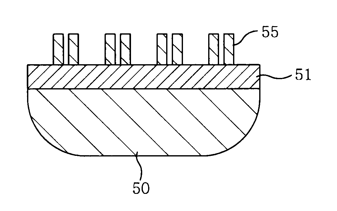
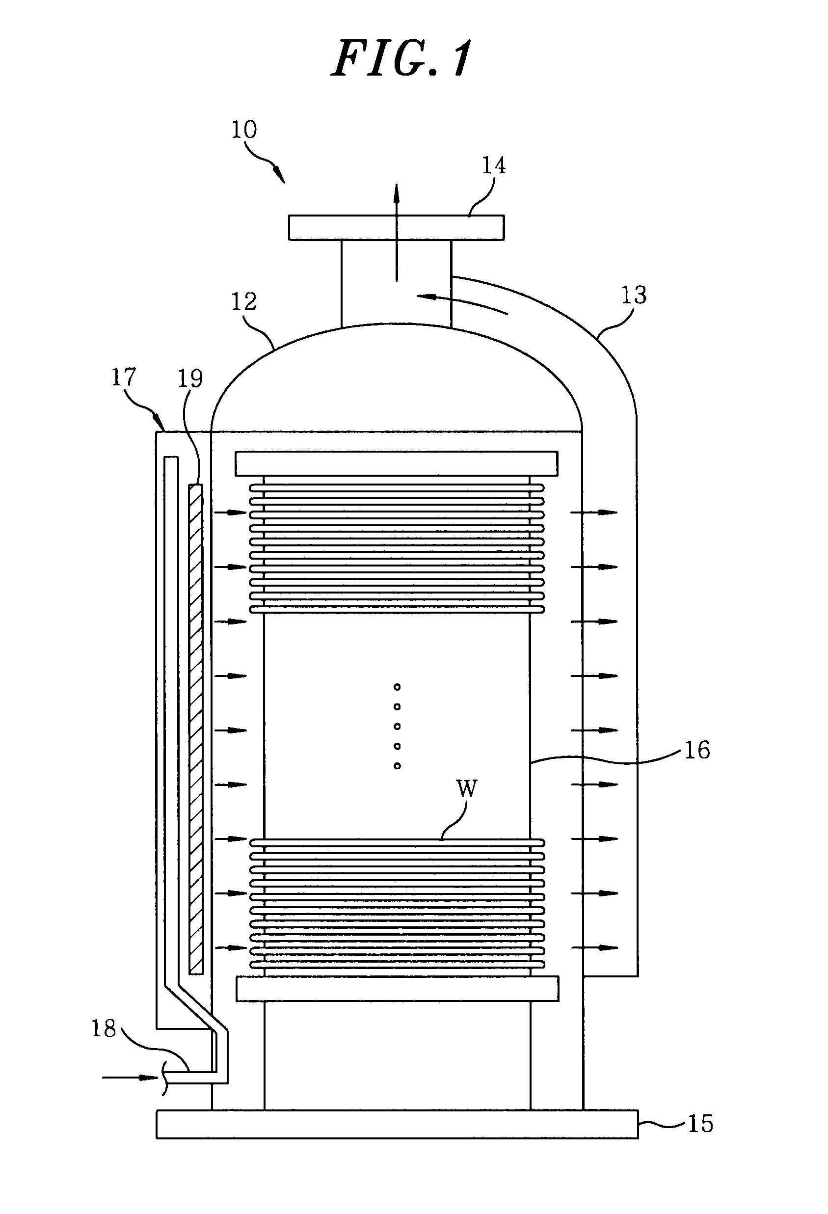
[0017]A substrate processing apparatus in which a substrate processing method in accordance with the embodiment of the present invention is carried out will be described first. The substrate processing apparatus is an apparatus (referred to as “deposition / trimming apparatus”) for trimming a line width of a line portion of an organic film of a semiconductor wafer W serving as a substrate, wherein, in the organic film, an opening pattern is formed while a reinforcement film is formed on a surface of the organic film by molecular layer deposition (MLD). Here, when a plasma is generated, a power can be increased to, e.g., approximately 500 W to 3,000 W.

[0018]FIG. 1 is a cross sectional view schematically showing a structure of a deposition / trimming apparatus 10 in which the substrate processing method in accordance with the embodiment of the present inv...


PUM


Abstract

A method for processing a substrate including a processing target layer and an organic film, include: a deposition/trimming process of forming a reinforcement film on a surface of the organic film and, at the same time, trimming a line width of a line portion of the organic film constituting an opening pattern. The deposition/trimming process includes an adsorption process for allowing a silicon-containing gas to be adsorbed onto the surface of the organic film and an oxidation process in which the line width of the organic film is trimmed while the adsorbed silicon-containing gas is converted into a silicon oxide film. A monovalent aminosilane is employed as the silicon-containing gas.

Description

CROSS-REFERENCE TO RELATED APPLICATIONS[0001]This application claims priority to Japanese Patent Application No. 2009-061139 filed on Mar. 13, 2009, the entire contents of which are incorporated herein by reference.FIELD OF THE INVENTION[0002]The present invention relates to a substrate processing method; and, more particularly, to a substrate processing method for making a fine line width of a line portion of an organic film in which an opening pattern is formed while forming a reinforcement film on a surface of the organic film serving as a mask layer.BACKGROUND OF THE INVENTION[0003]There has been disclosed a wafer for a semiconductor device where an impurity-containing oxide film, e.g., a tetra ethyl ortho silicate (TEOS) film, produced by a chemical vapor deposition (CVD) or the like; an electrically conductive film, e.g., a titanium nitride (TiN) film; a bottom anti-reflective coating (BARC) film; and a mask layer (photoresist film) are stacked in that order on a silicon subst...

Claims


Application Information

Patent Timeline
IPC IPC(8): H01L21/316
CPCH01J37/32082H01J37/32779H01L21/32139H01L21/0337H01L21/0273
Inventor KUSHIBIKI, MASATONISHIMURA, EIICHI
Owner TOKYO ELECTRON LTD
Why Eureka
Try Eureka