Method of manufacturing a semiconductor device

a manufacturing method and semiconductor technology, applied in semiconductor devices, semiconductor/solid-state device details, electrical devices, etc., can solve the problems of unwanted effect, unwanted etching, and increase the tendency of voids to form, and achieve the effect of simple and inexpensive new process

Inactive Publication Date: 2010-09-23
LAPIS SEMICON CO LTD
View PDF3 Cites 46 Cited by
  • Summary
  • Abstract
  • Description
  • Claims
  • Application Information

AI Technical Summary

Benefits of technology

[0016]The novel process is simple and inexpensive, particularly if the tungsten hexafluoride deposition source gas is also used as an etching ga

Problems solved by technology

Tungsten CVD is therefore usually carried out under region B conditions, but WF6 gas also has the unwanted effect of etching the deposited layer of tungsten, the substrate layer on which the tungsten is deposited, and the dielectric film in which the hole is formed.
Ideally, it should always be possible to fill holes with tungsten as in FIG. 3, without creating voids, by performing tungsten CVD under region B conditions, but as the dimensions of wiring traces and the diameter of via holes become increasingly small, or the holes become increasingly deep,

Method used


Image

  • Method of manufacturing a semiconductor device
  • Method of manufacturing a semiconductor device
  • Method of manufacturing a semiconductor device

Examples


first embodiment

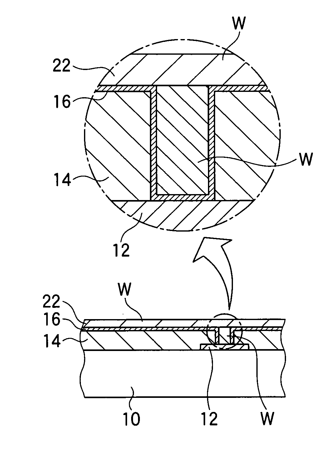
[0023]Referring to FIG. 4, the method of forming a semiconductor device according to the first embodiment begins from a semiconductor substrate 10 on which semiconductor circuit elements (not shown) and interconnection wiring 12, electrically coupled to the semiconductor circuit elements, are formed. A dielectric film 14 such as a layer of silicon oxide or a layer of borophosphosilicate glass (BPSG) is then formed, covering the interconnection wiring 12, and is selectively etched by photolithography and reactive ion etching to form holes 18 extending from the surface of the dielectric film 14 down to the underlying wiring layer or circuit element. Next an adhesion layer such as a layer of titanium nitride (TiN) is formed on the surface of the dielectric film 14 and the inner side and bottom walls of each hole 18.

[0024]Although the illustrated hole 18 leads to interconnection wiring 12, the novel process may also be applied in other configurations: for example, the hole 18 may lead t...

second embodiment

[0041]The second embodiment includes the steps already shown in FIGS. 4 to 8, which fill a hole 18 formed in a dielectric film 14 with tungsten and form a tungsten layer on the surface of the dielectric film 14, and two further steps, which will be described below.

[0042]Referring to FIG. 9, the next step is a second etching step that etches the tungsten layer deposited on the surface of the dielectric film 14 in the second deposition step. This etching step removes substantially all of the tungsten from the surface of the dielectric film 14.

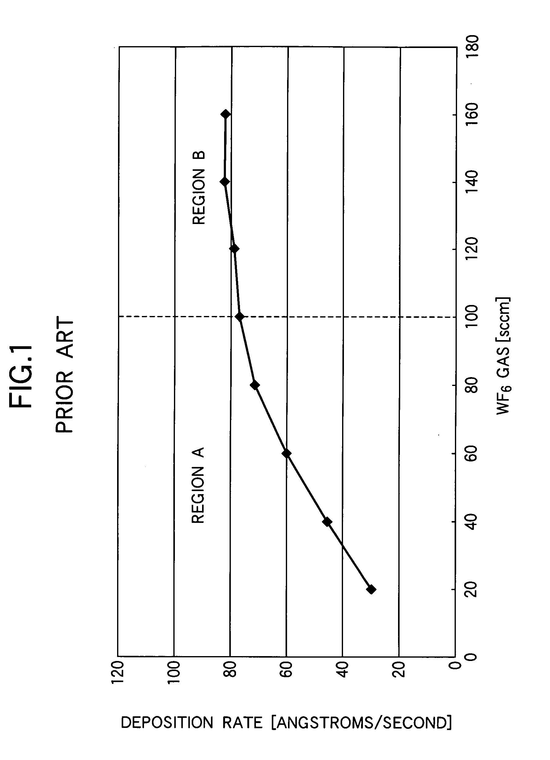
[0043]This second etching step is carried out in situ by halting the flow of hydrogen gas that was supplied during the second deposition step, reducing the WF6 gas flow to less than 100 sccm (region A), and using WF6 gas as an etching gas, without moving the semiconductor substrate 10 from the deposition chamber in which the first and second deposition steps were carried out. Exemplary conditions for this second etching step are a temperature of ...


PUM


Abstract

A semiconductor device manufacturing method includes a process for filling holes in a dielectric film with tungsten. The process deposits tungsten in the holes, partially etches the deposited tungsten, and then deposits additional tungsten in the holes. Voids that may be left by the first tungsten deposition step are made accessible by openings formed in the etching step, and are then filled in by the second tungsten deposition step. Tungsten hexafluoride may be used as both a deposition source gas and an etching gas, providing a simple and inexpensive process that is suitable for high-volume production.

Description

BACKGROUND OF THE INVENTION[0001]1. Field of the Invention[0002]The present invention relates to a method of manufacturing a semiconductor device, more particularly to a method of depositing tungsten in holes in a semiconductor device.[0003]2. Description of the Related Art[0004]Tungsten (W) is a conductive metal that is commonly used to fill the contact holes or via holes that pass through dielectric films to interconnect wiring traces in different wiring layers in semiconductor devices.[0005]The known methods of depositing tungsten include chemical vapor deposition (CVD), sputtering, and atomic layer epitaxy (ALE). The most widely used method is tungsten CVD, a description of which is given by Miyata in Japanese Patent Application Publication No. H10-209280. This method employs, for example, the reaction between tungsten hexafluoride gas (WF6) and hydrogen gas (H2) given by the following formula:WF6+3H2→W+6HF[0006]When this reaction is used to deposit tungsten in a hole under cond...

Claims


Application Information

Patent Timeline
IPC IPC(8): H01L21/768
CPCH01L21/76877H01L21/28556
Inventor TAKAHASHI, MASASHI
Owner LAPIS SEMICON CO LTD
Why Eureka
Try Eureka