Solar cell device

a solar cell and solar cell technology, applied in the field of solar cell devices, can solve the problems of limited thickness, conductive glass coated with tin oxide, major loss of ohmic energy, etc., and achieve the effect of low-grad

Active Publication Date: 2010-09-30
3GSOLAR PHOTOVOLTAICS
View PDF14 Cites 17 Cited by
  • Summary
  • Abstract
  • Description
  • Claims
  • Application Information

AI Technical Summary

Benefits of technology

[0050]According to still further features in the described preferred embodiments, the at least partially transparent conductive coating includes tin oxide, and the electrical resistance of the c...

Problems solved by technology

It is further argued that there might be significant cost savings over classical single crystal or polycrystalline silicon cells and even more recent thin-film photovoltaic cells, since these are all high cost and rely on expensive and often environmentally problematic raw materials, together with complex, costly, semiconductor industry processing equipment and production techniques.
These drawbacks include the use of vacuum deposition and laser methods, clean-room protocols, use of toxic hydrides such as silane, phosphine etc., as raw materials, and the use of toxic active-layer materials containing cadmium, selenium or tellurium.
The ohmic loss via the conductive glass coated with tin oxide is a major problem of such cells.
The tin oxide coating is extremely thin, being limited in thickness usually to below one micron due to the need to maintain a high light transmittance through to the dye/titania layer of the photoanode.
Moreover, tin oxide is only semi-conductive and is mechanically weak, such that the current takeoff is significantly limited by such a cell design.
Furthermore, the emphasis is on single cell construction with no advantage offered for construction of a multi-cell module.
Most significantly, the periphery (i.e., the sides) of the cel...

Method used


Image

  • Solar cell device
  • Solar cell device
  • Solar cell device

Examples


Embodiment Construction

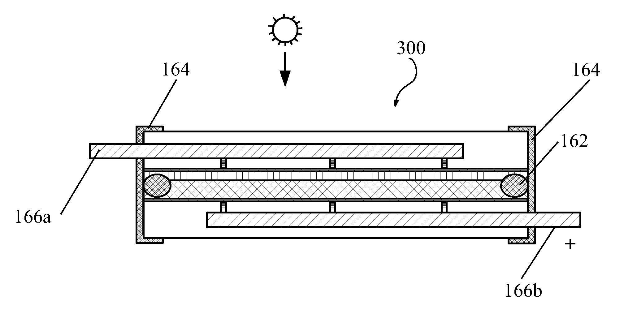
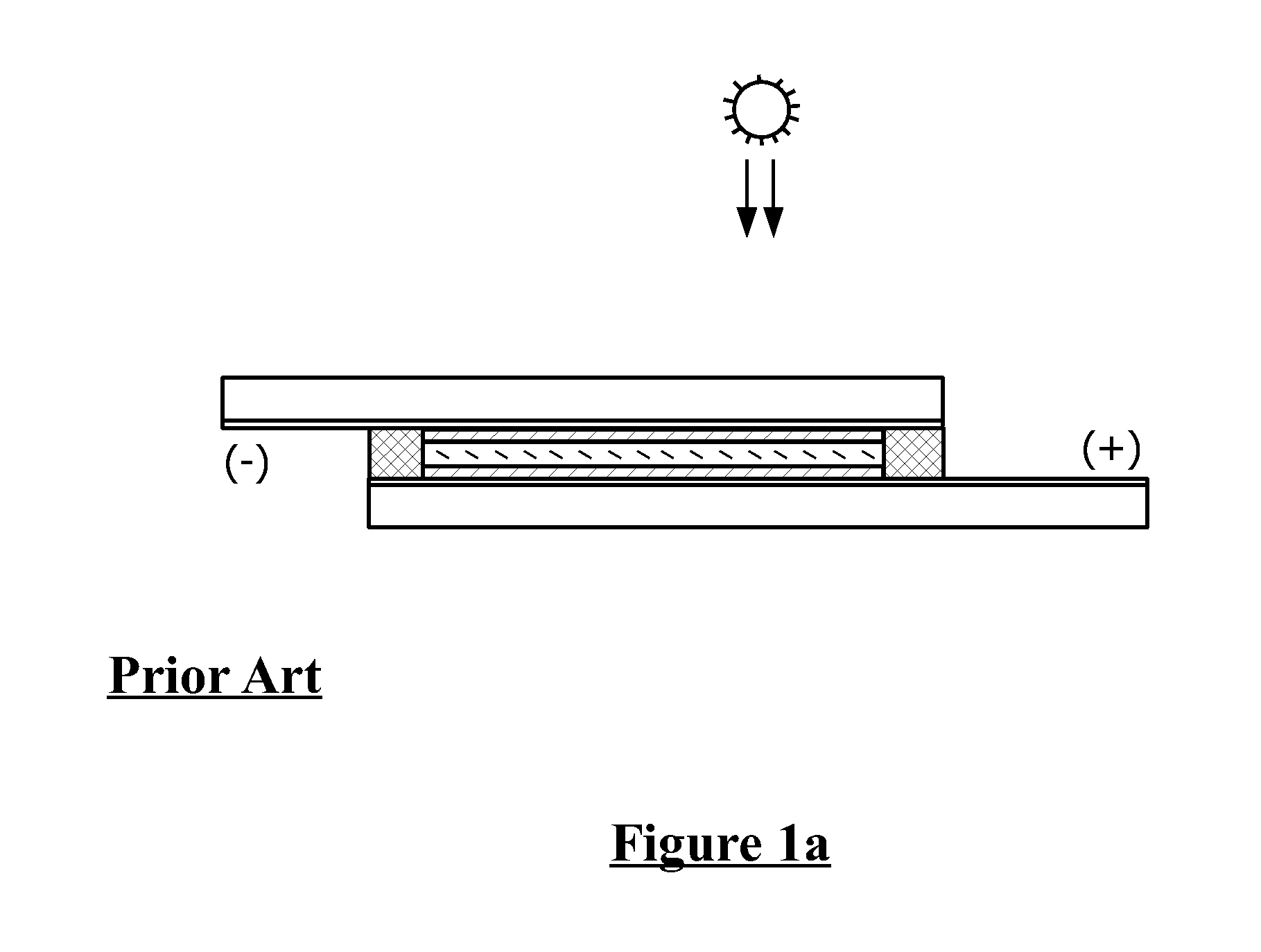
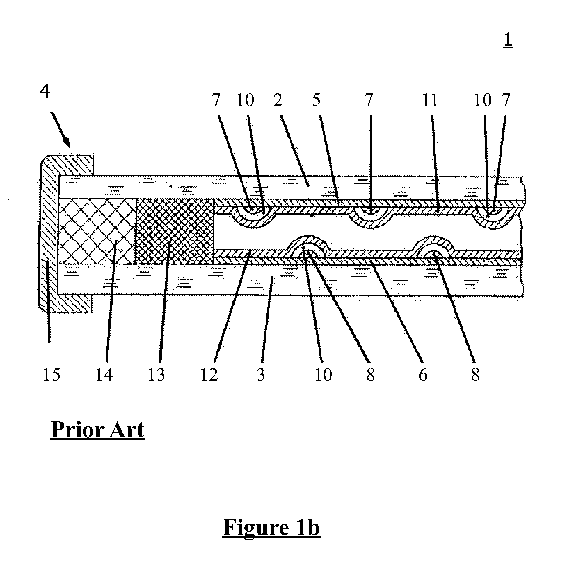
[0072]The principles and operation of the photovoltaic cells according to the present invention may be better understood with reference to the drawings and the accompanying description.

[0073]Before explaining at least one embodiment of the invention in detail, it is to be understood that the invention is not limited in its application to the details of construction and the arrangement of the components set forth in the following description or illustrated in the drawings. The invention is capable of other embodiments or of being practiced or carried out in various ways. Also, it is to be understood that the phraseology and terminology employed herein is for the purpose of description and should not be regarded as limiting.

[0074]The present invention overcomes these and other problems and paves the way to the manufacture of an efficient, commercially viable device. Various aspects and embodiments of the present invention are described hereinbelow:

[0075]One aspect of the present inven...


PUM


Abstract

A photovoltaic cell including: (a) a housing including an at least partially transparent cell wall having an interior surface; (b) an electrolyte, disposed within the cell wall, and containing an iodide based species; (c) a transparent electrically conductive coating disposed on the interior surface; (d) an anode disposed on the conductive coating, the anode including: (i) a porous film containing titania, the porous film adapted to make intimate contact with the iodide based species, and (ii) a dye, absorbed on a surface of the porous film, the dye and the porous film adapted to convert photons to electrons; (e) a cathode disposed on an interior surface of the housing, and disposed substantially opposite the anode; (f) electrically-conductive metallic wires, disposed at least partially within the cell, the wires electrically contacting the anode and the electrically conductive coating, and (g) a second electrically conductive coating including an inorganic binder and an inorganic electrically conductive filler, the second coating bridging between and electrically communicating between each of the wires and the transparent coating, the wires adapted to boost collection of a current generated by the cell.

Description

CROSS-REFERENCE TO RELATED APPLICATIONS[0001]This application is a continuation-in-part (CIP) application of U.S. patent application Ser. No. 10 / 754,584, filed Jan. 12, 2004, which draws priority from Israel Patent Application Ser. No. 153,895, filed Jan. 12, 2003, a continuation-in-part (CIP) application of U.S. patent application Ser. No. 12 / 618,741, filed Nov. 15, 2009, which draws priority from PCT Application No. IL2008 / 000671, filed May 15, 2008, which draws priority from U.S. Provisional Patent Application Ser. No. 60 / 917,941, filed May 15, 2007, and a continuation-in-part (CIP) application of U.S. patent application Ser. No. 12 / 744,914, filed May 26, 2010, which draws priority from PCT Application No. IL2008 / 001550, filed Nov. 26, 2008, which draws priority from U.S. Provisional Patent Application Ser. No. 60 / 990,307, filed Nov. 27, 2007, all of which are hereby incorporated by reference for all purposes as if fully set forth herein.FIELD AND BACKGROUND OF THE INVENTION[0002...

Claims


Application Information

Patent Timeline
IPC IPC(8): H01L31/00
CPCH02S40/44Y02E10/60Y02E10/50
Inventor GOLDSTEIN, JONATHAN
Owner 3GSOLAR PHOTOVOLTAICS
Why Eureka
Try Eureka