Structure and fabrication of field-effect transistor using empty well in combination with source/drain extensions or/and halo pocket

a field-effect transistor and halo pocket technology, applied in the field of field-effect transistors, can solve the problems of weakened analog performance, difficult to integrate choi's process into a larger semiconductor process, and the inability to control the operation of the igfet gate electrode, etc., to achieve the effect of facilitating the igfet fabrication, reducing the doping of the s/d extension, and facilitating the setting of the threshold voltage of the ig

Active Publication Date: 2010-09-30
NAT SEMICON CORP
View PDF27 Cites 10 Cited by
  • Summary
  • Abstract
  • Description
  • Claims
  • Application Information

AI Technical Summary

Benefits of technology

[0039]Some desirable IGFET performance characteristics, e.g., threshold voltages of low magnitude, are more readily achieved with symmetric IGFETs when they utilize empty-well regions. The performance characteristics of asymmetric IGFETs are readily enhanced by using empty-well regions. On the other hand, other desirable IGFET performance characteristics, e.g., low-off-state current leakage and threshold voltages of nominal magnitude, are more readily achieved with symmetric IGFETs when they employ filled-well regions. The combination of filled-well IGFETs with empty-well IGFETs configured according to the invention makes the semiconductor fabrication platform extremely versatile.
[0043]In one aspect of the invention, each S / D zone contains a main S / D portion and a more lightly doped lateral S / D extension laterally continuous with the main S / D portion and extending laterally under the gate electrode. The channel zone is terminated by the S / D extensions along the upper semiconductor surface. Usage of lateral S / D extensions, especially for the S / D zone acting as the IGFET's drain, generally reduces hot carrier injection into the IGFET's gate dielectric layer. Undesired threshold-voltage drift with operational time is thereby reduced. The IGFET operates very efficiently. In a symmetric implementation of the IGFET, the empty well facilitates setting the IGFET's threshold voltage at a low magnitude.
[0044]The specified S / D zone, i.e., the S / D zone having the vertical doping profile which establishes the present IGFET as an empty-well IGFET, is typically the second S / D zone. Another implementation of the IGFET is an asymmetric device in which the S / D extension of the second S / D zone is more lightly doped than the S / D extension of the first S / D zone. Additionally or alternatively, the S / D extension of the second S / D zone extends deeper below the upper semiconductor surface than the S / D extension of the first S / D zone. Reducing the doping of the S / D extension of the second S / D zone or / and increasing the depth of the S / D extension of the second S / D zone generally causes hot carrier injection in the gate dielectric layer to be reduced further. Threshold-voltage drift is likewise reduced further.
[0045]In another aspect of the invention, a pocket portion of the body material more heavily doped than laterally adjacent material of the body material extends along the first S / D zone into the channel zone. The pocket portion preferably extends largely along only the first S / D zone so that the channel zone is asymmetric with respect to the S / D zones. With the first S / D zone acting as the source, the presence of the pocket portion helps to avoid bulk punchthrough and consequent inability to control the IGFET through its gate electrode. The empty-well IGFET of the invention typically combines the S / D extensions with the pocket portion.

Problems solved by technology

When surface or bulk punchthrough occurs, the operation of the IGFET cannot be controlled with its gate electrode.
However, Choi's coupling of the formation of gate electrode 46 with the formation of source / drain extensions 26E and 28E in the process of FIG. 10 is laborious and could make it difficult to incorporate Choi's process into a larger semiconductor process that provides other types of IGFETs.
Although it would be economically attractive to utilize the same transistors for the analog and digital blocks, doing so would typically lead to weakened analog performance.
Many requirements imposed on analog IGFET performance conflict with the results of digital scaling.
Hence, linearity demands on analog transistors are very high.
Because the resultant dimensional spreads are inherently large, parameter matching in digital circuitry is often relatively poor.

Method used


Image

  • Structure and fabrication of field-effect transistor using empty well in combination with source/drain extensions or/and halo pocket
  • Structure and fabrication of field-effect transistor using empty well in combination with source/drain extensions or/and halo pocket
  • Structure and fabrication of field-effect transistor using empty well in combination with source/drain extensions or/and halo pocket

Examples


Embodiment Construction

List of Contents

[0100]A. Reference Notation and Other Preliminary Information

[0101]B. Complementary-IGFET Structures Suitable for Mixed-signal Applications

[0102]C. Well Architecture and Doping Characteristics

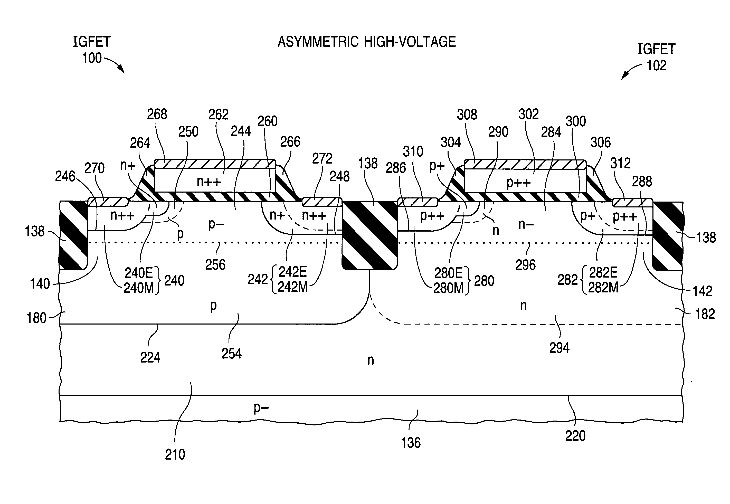
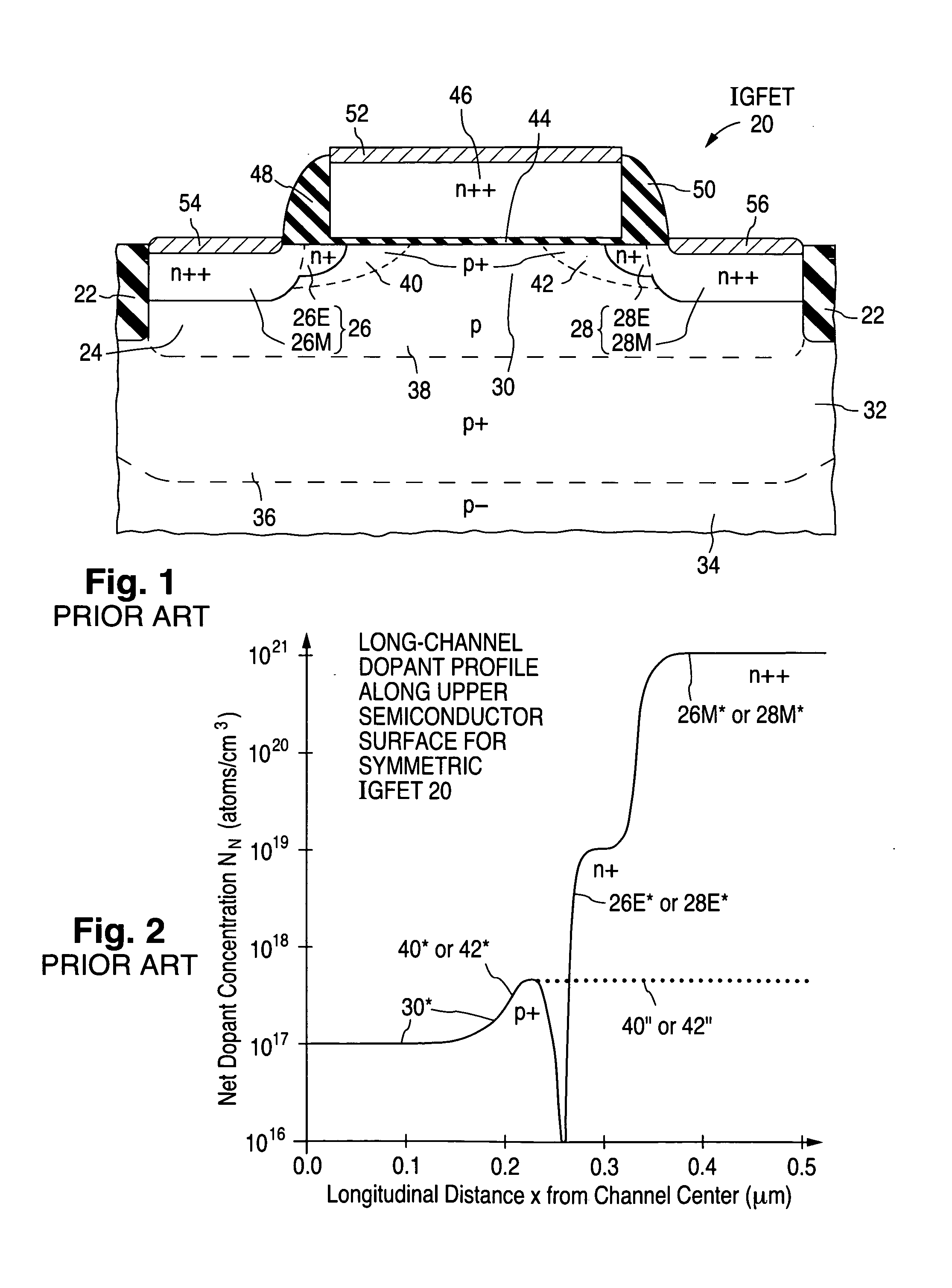
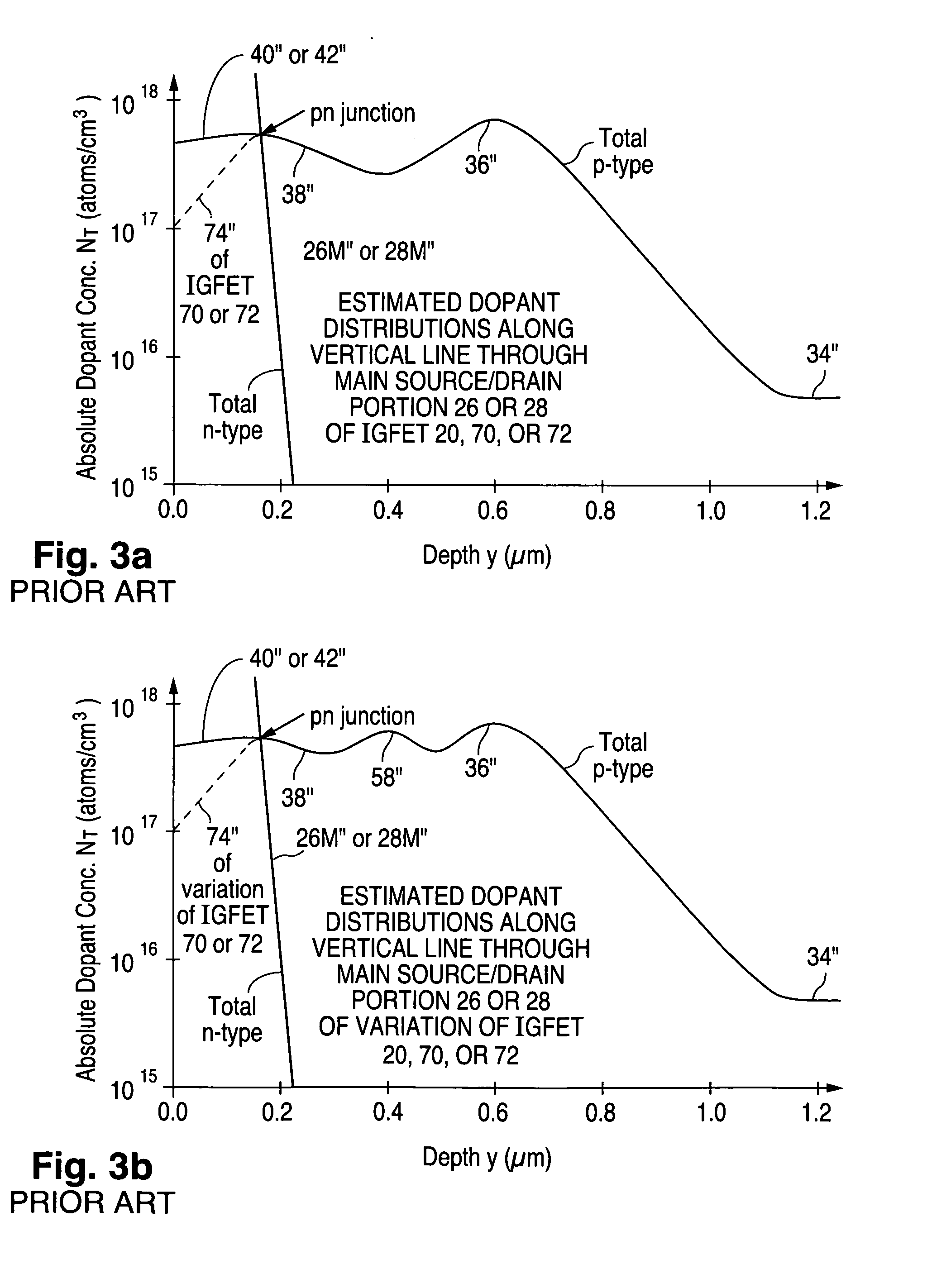
[0103]D. Asymmetric High-voltage IGFETs[0104]D1. Structure of Asymmetric High-voltage N-channel IGFET[0105]D2. Source / Drain Extensions of Asymmetric High-voltage N-channel IGFET[0106]D3. Different Dopants in Source / Drain Extensions of Asymmetric High-voltage N-channel IGFET[0107]D4. Dopant Distributions in Asymmetric High-voltage N-channel IGFET[0108]D5. Structure of Asymmetric High-voltage P-channel IGFET[0109]D6. Source / Drain Extensions of Asymmetric High-voltage P-channel IGFET[0110]D7. Different Dopants in Source / Drain Extensions of Asymmetric High-voltage P-channel IGFET[0111]D8. Dopant Distributions in Asymmetric High-voltage P-channel IGFET[0112]D9. Common Properties of Asymmetric High-voltage IGFETs[0113]D10. Performance Advantages of Asymmetric High-voltage IGFETs[0114]...


PUM


Abstract

Insulated-gate field-effect transistors (“IGFETs”), both symmetric and asymmetric, suitable for a semiconductor fabrication platform that provides IGFETs for analog and digital applications, including mixed-signal applications, utilize empty-well regions in achieving high performance. A relatively small amount of semiconductor well dopant is near the top of each empty well. Each IGFET (100, 102, 112, 114, 124, or 126) has a pair of source / drain zones laterally separated by a channel zone of body material of the empty well (180, 182, 192, 194, 204, or 206). A gate electrode overlies a gate dielectric layer above the channel zone. Each source / drain zone (240, 242, 280, 282, 520, 522, 550, 552, 720, 722, 752, or 752) has a main portion (240M, 242M, 280M, 282M, 520M, 522M, 550M, 552M, 720M, 722M, 752M, or 752M) and a more lightly doped lateral extension (240E, 242E, 280E, 282E, 520E, 522E, 550E, 552E, 720E, 722E, 752E, or 752E). Alternatively or additionally, a more heavily doped pocket portion (250 or 290) of the body material extends along one of the source / drain zones. When present, the pocket portion typically causes the IGFET to be an asymmetric device.

Description

CROSS-REFERENCE TO RELATED APPLICATIONS[0001]This application is related to the following U.S. patent applications all filed on the same date as this application: U.S. patent application Ser. No. ______ (Bulucea et al.), attorney docket no. NS-7005 US, U.S. patent application Ser. No. ______ (Bulucea et al.), attorney docket no. NS-7040 US, U.S. patent application Ser. No. ______ (Parker et al.), attorney docket no. NS-7192 US, U.S. patent application Ser. No. ______ (Bahl et al.), attorney docket no. NS-7210 US, U.S. patent application Ser. No. ______ (Yang et al.), attorney docket no. NS-7307 US, U.S. patent application Ser. No. ______ (Yang et al.), attorney docket no. NS-7313 US, U.S. patent application Ser. No. ______ (Bulucea et al.), attorney docket no. NS-7434 US, U.S. patent application Ser. No. ______ (French et al.), attorney docket no. NS-7435 US, U.S. patent application Ser. No. ______ (Bulucea et al.), attorney docket no. NS-7436 US, and U.S. patent application Ser. No...

Claims


Application Information

Patent Timeline
Patent Type & Authority Applications(United States)
IPC IPC(8): H01L29/78H01L21/265H01L21/336
CPCH01L21/26513H01L29/7835H01L21/26586H01L21/823807H01L21/823814H01L21/823892H01L27/0922H01L29/0653H01L29/0847H01L29/1045H01L29/105H01L29/1083H01L29/518H01L29/665H01L29/66659H01L29/7833H01L21/2652H01L21/2658
Inventor BULUCEA, CONSTANTINYANG, JENG-JIUNFRENCH, WILLIAM D.BAHL, SANDEEP R.PARKER, D. COURTNEY
Owner NAT SEMICON CORP
Why Eureka
Try Eureka