Deconvolution-based capacitive touch detection circuit and method

a capacitive touch and detection circuit technology, applied in the direction of resistance/reactance/impedence, measurement devices, instruments, etc., can solve the problems of inconvenient capacitance measurement times, time required for capacitance measurement, and modifies the cross-coupling capacitance, etc., to facilitate simultaneous driving of multiple rows, facilitate the effect of simultaneous driving multiple rows, and convenient operation

Inactive Publication Date: 2010-09-30
INTEL CORP
View PDF17 Cites 59 Cited by
  • Summary
  • Abstract
  • Description
  • Claims
  • Application Information

AI Technical Summary

Benefits of technology

[0024]It is another object of the invention to provide a high programmable capacitance measurement system capable of compensating manufacturing variations of integrated circuit variations within wafer lots and / or individual IC devices within a single wafer.
[0025]It is another object of the invention to provide a digital capacitance measurement system and method that allows simultaneous driving of multiple rows of a touch screen panel without overdriving or saturating an amplifier which a column signal generated as a result of the simultaneous driving of multiple rows.
[0026]It is another object of the invention to provide a digital capacitance measurement system and method that facilitates simultaneous driving of multiple rows of a touch screen panel without over driving or saturating an amplifier which receives a column signal generated as a result of the simultaneous driving of multiple rows by convoluting / superpositioning charge transfer from the multiple rows into the column signal and subsequently deconvoluting the digitized representation of the column signal.
[0027]It is another object of the invention to provide a digital capacitance measurement system and method that substantially reduces the digital processing requirement relative to the processing requirements of the prior art touch screen panel products by approximately an order of magnitude, and thereby provide a much smaller, faster, more economical touch screen controller than the prior art.

Problems solved by technology

The presence or movement of a user's finger in the vicinity of the electric field associated with the cross-coupling capacitance in the touch screen disturbs or impedes the electric field and therefore modifies the cross-coupling capacitance.
A problem of the above described prior art is that the time required for the capacitance measurement is time-varying in the sense that a lower value of the capacitance CSENij requires less counting time by timer capture register 7, whereas a higher value of the capacitance CSENij requires more counting time by timer capture register 7.
The widely variable capacitance measurement times may be inconvenient for a user.
Also, the system is quite susceptible to noise because comparator 6 in Prior Art FIG. 1B is connected via CSAMPLE during the entire capacitance measurement process.
Another problem of the above described prior art is that it is unsuitable for applications in which a small, inexpensive, low power touch screen controller circuit is needed because of the complexity of the above described prior art.

Method used


Image

  • Deconvolution-based capacitive touch detection circuit and method
  • Deconvolution-based capacitive touch detection circuit and method
  • Deconvolution-based capacitive touch detection circuit and method

Examples


Embodiment Construction

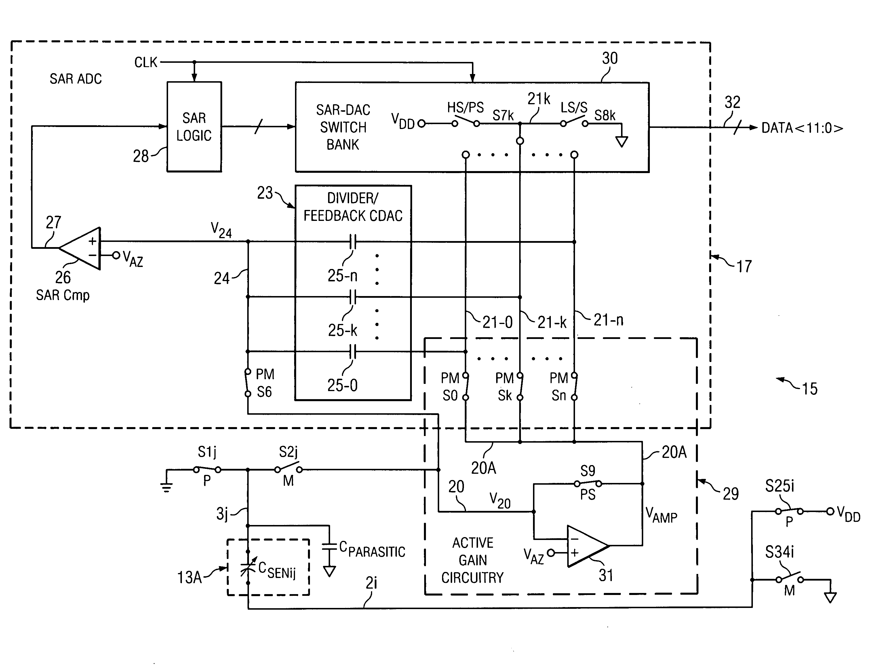
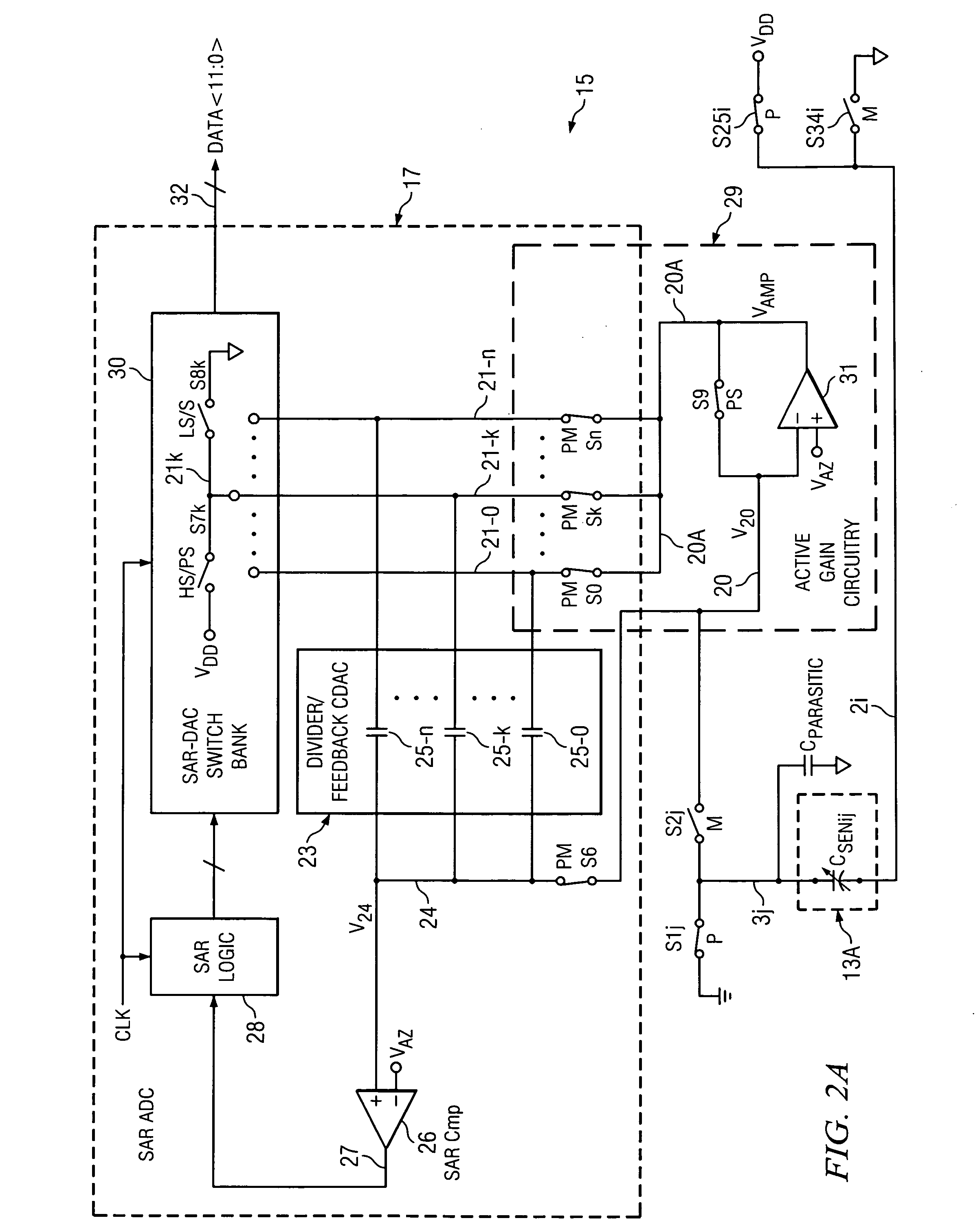
[0061]FIG. 2A shows a single-ended (i.e., not differential) embodiment of an embedded SAR based active capacitance measurement system 15 of the present invention which provides high capacitance measurement sensitivity, a wide range of parasitic capacitance, and a wide range of capacitance to be measured. Capacitance measurement system 15 includes active gain circuitry 29 and a SAR (successive approximation register) type of ADC (analog-to-digital converter) 17. Active gain circuitry 29 is coupled to effectuate measurement of touch screen capacitance CSENij where CSENij can be the cross-coupling capacitance in external touchscreen panel 13A (which can be similar to the touch screen panel shown in Prior Art FIGS. 1A and 1B). The capacitance CSENij is typically decreased (depending on the particular panel or touch button configuration) by the presence of a human finger (or other conductive probe) in the electric field associated with capacitance CSENij.

[0062]In FIG. 2A, a cross-couplin...


PUM


Abstract

A capacitance measuring system includes analog-digital circuitry (15) coupled to row conductors (2i) and column conductors (3i) of a touch screen panel (13A) for producing a first digital signal (DATA) representative of cross-coupling capacitances (CSENij). Row drive circuitry (45) superimposes charge transfers from cross-coupling capacitances of the row conductors to a first column conductor to cause the first digital signal to be a convoluted signal. Calibration circuitry (39,40) subtracts base line data from the first digital signal to produce a second digital signal (ΔDATA) representing touch-induced capacitance change values (ΔCSENIJ). A deconvolution circuit (44) deconvolutes the second digital signal to produce a digital output (58) representing a magnitude map of the touch-induced capacitance change values.

Description

CROSS REFERENCE TO RELATED APPLICATION[0001]This application is a continuation-in-part of commonly assigned pending patent application Ser. No. 12 / 383,696 filed on Mar. 27, 2009, entitled “EMBEDDED SAR BASED ACTIVE GAIN CAPACITANCE MEASUREMENT SYSTEM AND METHOD” by Ronald F. Cormier, Jr., and incorporated herein by reference.BACKGROUND OF THE INVENTION[0002]The present invention relates generally to circuits and techniques for measurement of capacitance, and more particularly to improvements in circuits and techniques adapted for processing digital signals generated by the touch screen controller circuitry that scans a touch screen panel.[0003]Touch screen controller circuits for use in touch screen applications have generally included digital controller circuitry and analog circuitry for detecting / measuring the presence of capacitance if a user touches a point on a touch screen. The presence or movement of a user's finger in the vicinity of the electric field associated with the cr...

Claims


Application Information

Patent Timeline
Patent Type & Authority Applications(United States)
IPC IPC(8): G01R27/26
CPCG06F3/044G06F3/0446
Inventor CORMIER, JR., RONALD F.SNEDEKER, MICHAEL D.
Owner INTEL CORP
Why Eureka
Try Eureka