Coated pcbn cutting insert, coated pcbn cutting tool using such coated pcbn cutting insert, and method for making the same

a technology of pcbn cutting insert and coating, which is applied in the direction of superimposed coating process, other chemical processes, natural mineral layered products, etc., can solve the problems of reducing tensile stress, reducing tensile stress, and reducing tensile stress

Active Publication Date: 2010-10-07
KENNAMETAL INC
View PDF33 Cites 22 Cited by
  • Summary
  • Abstract
  • Description
  • Claims
  • Application Information

AI Technical Summary

Problems solved by technology

The presence of the tensile stress is detrimental to the adhesion of the CVD coating scheme.
These patent documents do not disclose the actual implementation of a post-coating treatment to a coating that has been applied to the surface of a PcBN body (or PcBN cutting insert) resulting in a reduction of the tensile stress or a conversion of the stress to compressive stress in the coating layer(s), as well as a smoothening of the outer coating layer.

Method used


Image

  • Coated pcbn cutting insert, coated pcbn cutting tool using such coated pcbn cutting insert, and method for making the same
  • Coated pcbn cutting insert, coated pcbn cutting tool using such coated pcbn cutting insert, and method for making the same
  • Coated pcbn cutting insert, coated pcbn cutting tool using such coated pcbn cutting insert, and method for making the same

Examples


Embodiment Construction

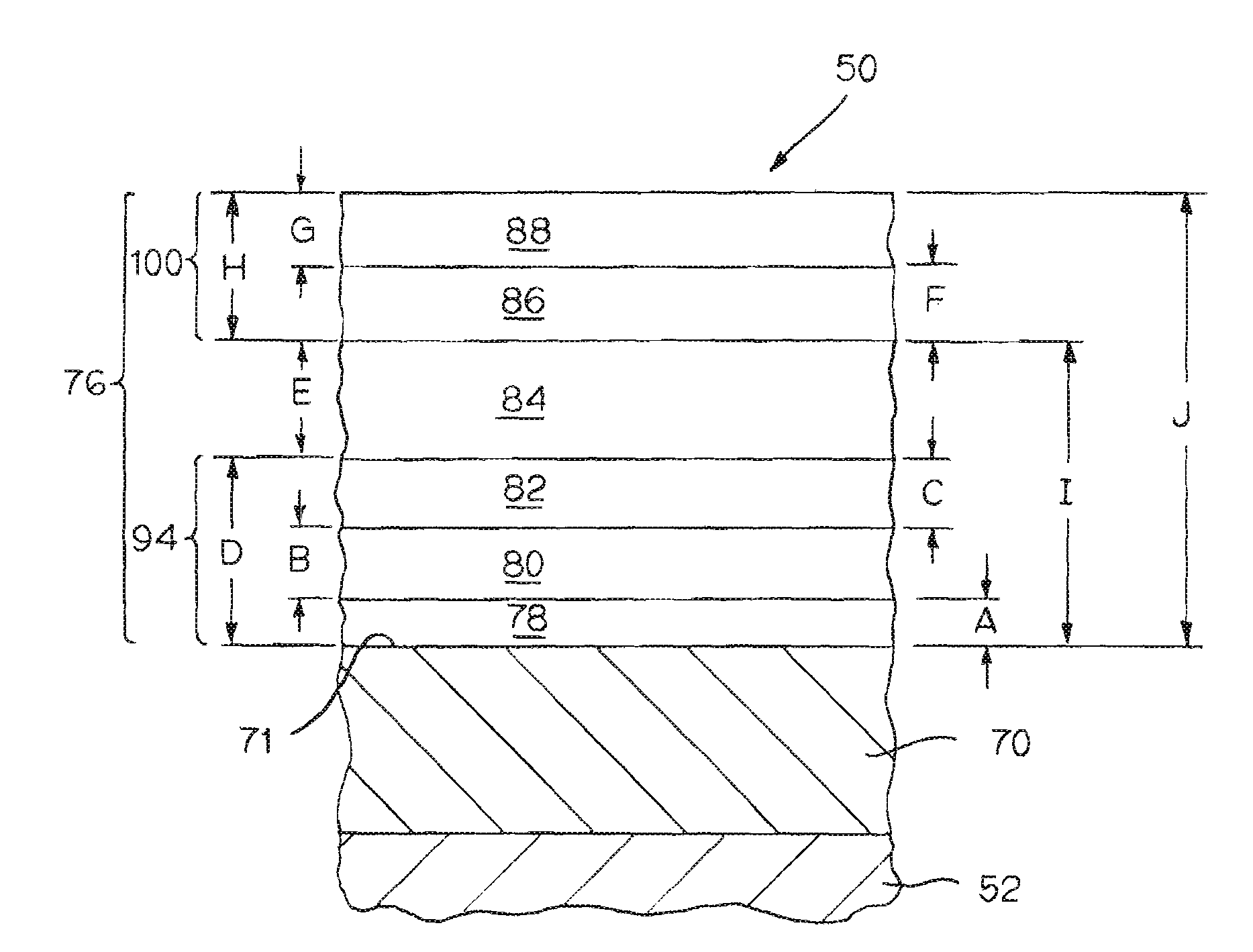
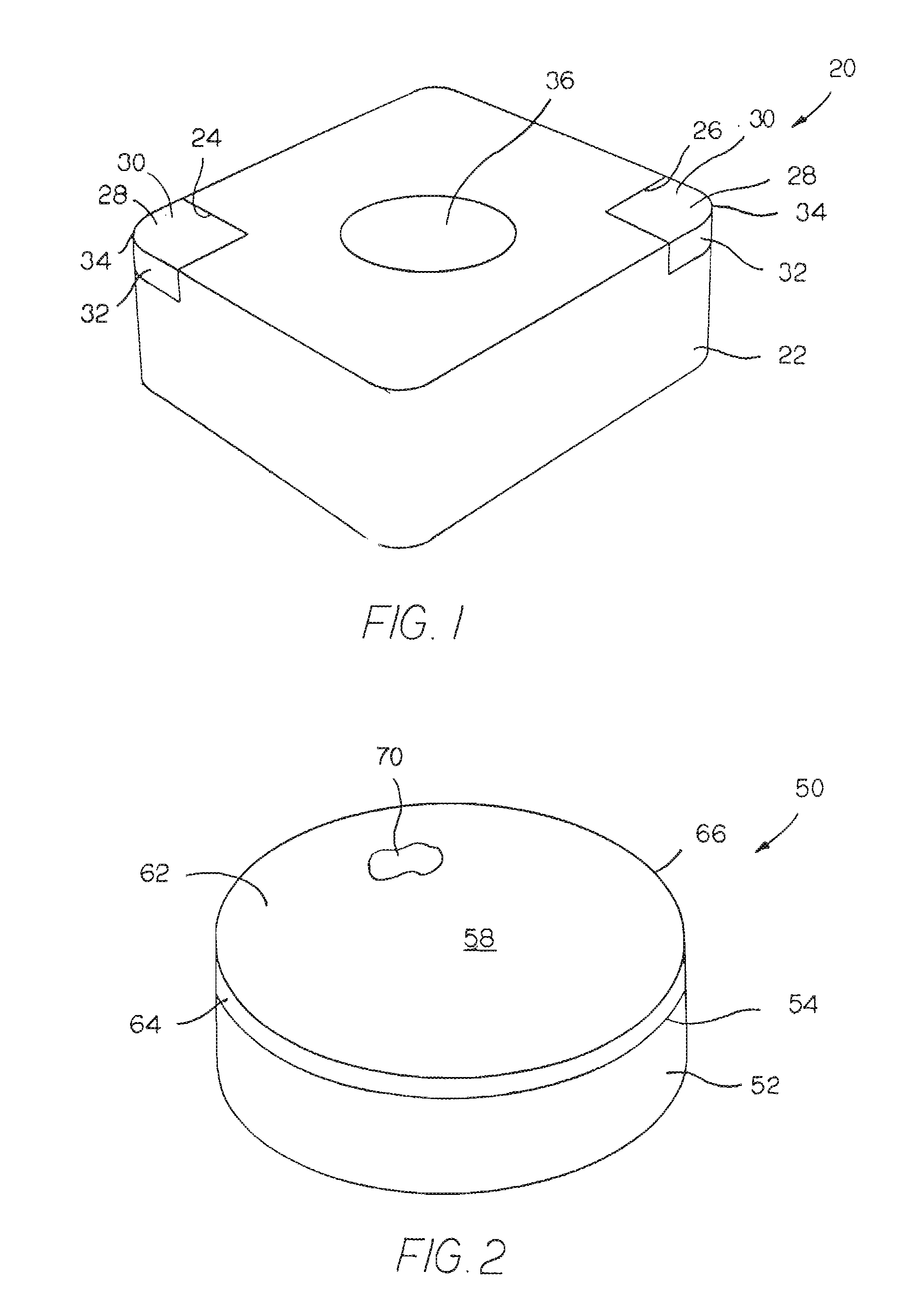
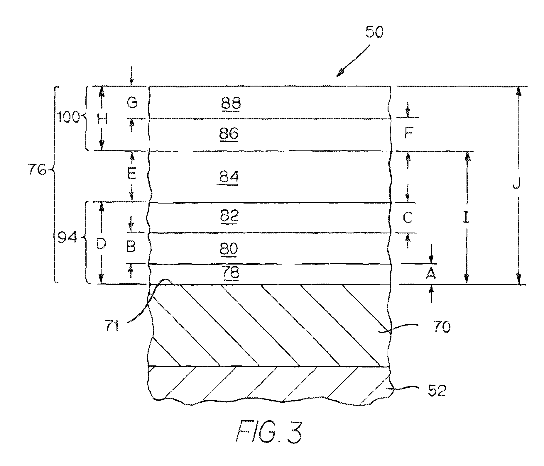
[0027]Referring to the drawings, FIG. 1 shows a specific embodiment of a coated PcBN cutting tool, which is generally designated as 20, useful for the removal of material from a workpiece, e.g., chipforming machining of a workpiece. FIG. 2 shows another specific embodiment of a coated PcBN cutting tool, which is generally designated as 50, useful for the removal of material from a workpiece, e.g., chipforming machining of a workpiece.

[0028]In reference to the chipforming machining operation, material removal operations generate chips of the workpiece material. Publications that pertain to machining establish this fact. For example, the book Machine Shop Practice [Industrial Press Inc., New York, N.Y. (1981)] by Moltrecht, presents at pages 199-204 a description, inter alia, of chip formation, as well as different kinds of chips (i.e., continuous chip, discontinuous chip, segmental chip). Moltrecht reads [in part] at pages 199-200:[0029]When the cutting tool first makes contact with ...


PUM

PropertyMeasurementUnit
tensile stressaaaaaaaaaa

Abstract

A coated polycrystalline cubic boron nitride cutting insert useful in a cutting tool for removing material from a workpiece, and a method for making the same. The cutting insert including a polycrystalline cubic boron nitride substrate with a rake surface and at least one flank surface, and a cutting edge formed at the juncture between the rake surface and the flank surface. A wear-resistant coating scheme is on the polycrystalline cubic boron nitride substrate. The wear-resistant coating scheme includes the following coating layers. An inner coating layer region is on at least some of the rake surface and at least some of the flank surface of the polycrystalline cubic boron nitride substrate. An alumina-containing coating layer region, which has at least one exposed alumina coating layer, is on the inner coating layer region. The exposed alumina coating layer exhibiting a post-blasted stress condition with stress ranging between about 50 MPa (tensile stress) and about −2 GPa (compressive stress) as measured by XRD using the Psi tilt method and the (024) reflection of alumina. The exposed coating layer is the result of wet blasting an outer titanium-containing coating layer from the surface of the alumina-containing coating layer region.

Description

CROSS-REFERENCE TO EARLIER CO-PENDING PATENT APPLICATION[0001]This patent application is a continuation-in-part of earlier filed and co-pending U.S. patent application Ser. No. 12 / 057,564 filed Mar. 28, 2008 by Zhigang Ban, Mark J. Rowe, Yixiong Liu, Alfred S. Gates, Jr., Kent P. Mizgalski and Mark S. Greenfield for a CUTTING INSERT WITH A WEAR-RESISTANT COATING SCHEME EXHIBITING WEAR INDICATION AND METHOD OF MAKING THE SAME, which is a continuation-in-part of earlier-filed and co-pending U.S. patent application Ser. No. 11 / 823,679 filed on Jun. 28, 2007 by Zhigang Ban, Mark J. Rowe, Yixiong Liu, and Alfred S. Gates, Jr. for a CUTTING INSERT WITH A WEAR-RESISTANT COATING SCHEME EXHIBITING WEAR INDICATION AND METHOD OF MAKING THE SAME. Applicants herein (Zhigang Ban, and Yixiong Liu) claim under the United States Patent Statute (Title 35, United States Code) including 35 U.S.C. §120 the benefit of the filing date of each one of such earlier patent applications; namely, U.S. patent ap...

Claims


Application Information

Patent Timeline
Patent Type & Authority Applications(United States)
IPC IPC(8): B32B9/04C23C16/00
CPCB23B27/141B23B2226/125B23B2228/10B23B2260/144C23C16/30C23C28/044C23C16/36C23C16/403C23C16/56C23C30/005C23C16/34C04B41/89C04B41/009C04B41/52C04B35/5831C04B41/4531C04B41/5068C04B41/5061C04B41/5041C04B41/5031C23C16/40C23C28/00B23B27/14
Inventor BAN, ZHIGANGLIU, YIXIONG
Owner KENNAMETAL INC
Why Eureka
Try Eureka