Back diffusion suppression structures

a technology of diffusion suppression and back diffusion, which is applied in the direction of basic electric elements, electrical equipment, and semiconductor devices, etc., can solve the problems of low conductivity in the region between the gate and the ohmic contact, time dependent changes in threshold and conductivity of the device, and higher threshold voltage under the ga

Active Publication Date: 2010-10-14
EFFICIENT POWER CONVERSION CORP
View PDF5 Cites 90 Cited by
  • Summary
  • Abstract
  • Description
  • Claims
  • Application Information

AI Technical Summary

Problems solved by technology

There are several disadvantages of the conventional enhancement mode GaN transistors shown in FIG. 1.
This leads to higher threshold voltage under the gate and lower conductivity in the region between the gate and the ohmic contacts.
In addition, the charging and dischar

Method used


Image

  • Back diffusion suppression structures
  • Back diffusion suppression structures
  • Back diffusion suppression structures

Examples


Embodiment Construction

[0024]In the following detailed description, reference is made to certain embodiments. These embodiments are described with sufficient detail to enable those skilled in the art to practice them. It is to be understood that other embodiments may be employed and that various structural, logical, and electrical changes may be made.

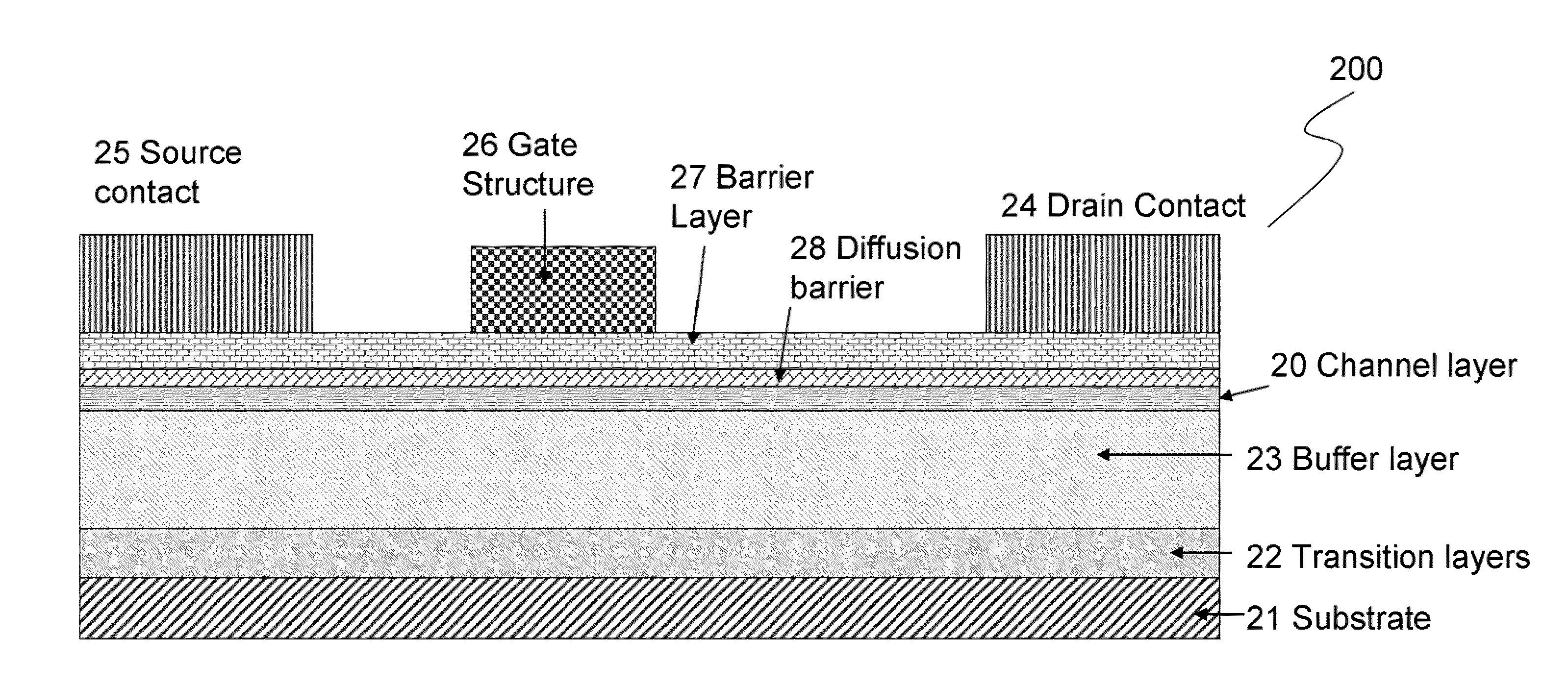
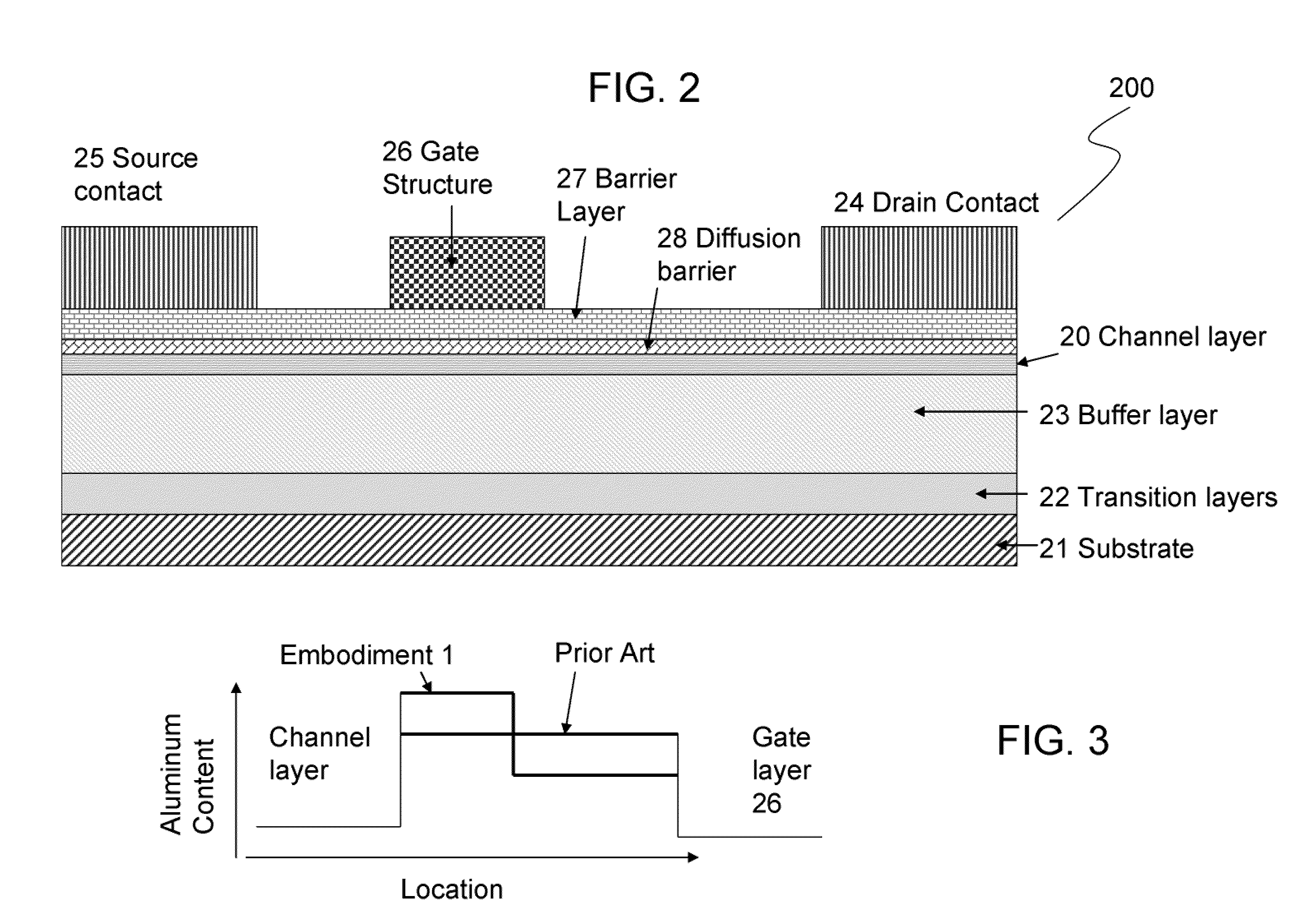
[0025]Embodiments of the invention described herein relate to an enhancement mode GaN transistor with a diffusion barrier that prevents Mg atoms from diffusing through the crystal into the active regions of the device. The embodiments are based on the addition of a diffusion barrier and / or a graded doping profile to reduce or eliminate the diffusion of dopant atoms (e.g., Mg). In one embodiment of the current invention, a thin AlN, or high Al content AlGaN layer is deposited above the primary channel layer to block the back diffusion of Mg into this region. In another embodiment of the invention, a thin AlN or high Al AlGaN layer is deposited within or above ...


PUM


Abstract

An enhancement-mode GaN transistor, the transistor having a substrate, transition layers, a buffer layer comprised of a III Nitride material, a barrier layer comprised of a III Nitride material, drain and source contacts, a gate containing acceptor type dopant elements, and a diffusion barrier comprised of a III Nitride material between the gate and the buffer layer.

Description

CROSS REFERENCE TO RELATED APPLICATIONS[0001]This application claims priority from U.S. Provisional Application No. 61 / 167,817, filed on Apr. 8, 2009, which is hereby incorporated by reference in its entirety.FIELD OF THE INVENTION[0002]The present invention relates to the field of enhancement mode gallium nitride (GaN) transistors. More particularly, the invention relates to an enhancement mode GaN transistor with a diffusion barrier.BACKGROUND OF THE INVENTION[0003]Gallium nitride (GaN) semiconductor devices are increasingly desirable for power semiconductor devices because of their ability to carry large current and support high voltages. Development of these devices has generally been aimed at high power / high frequency applications. Devices fabricated for these types of applications are based on general device structures that exhibit high electron mobility and are referred to variously as heterojunction field effect transistors (HFET), high electron mobility transistors (HEMT), ...

Claims


Application Information

Patent Timeline
IPC IPC(8): H01L29/772H01L21/20H01L21/306
CPCH01L29/1066H01L29/2003H01L29/7786H01L29/66462H01L29/475
Inventor LIDOW, ALEXANDERBEACH, ROBERTZHAO, GUANG Y.CAO, JIANJUN
Owner EFFICIENT POWER CONVERSION CORP
Why Eureka
Try Eureka