Semiconductor device

Inactive Publication Date: 2010-10-14
RENESAS ELECTRONICS CORP
View PDF7 Cites 28 Cited by
  • Summary
  • Abstract
  • Description
  • Claims
  • Application Information

AI Technical Summary

Benefits of technology

[0023]The following is a brief description of the gist of effect obtained by the representative elements of the invention laid open in this application:
[0024]According to atypical embodiment, it is possible to enhance the characteristics of a semiconductor d

Problems solved by technology

When in a light emitting device for flash photography, the components comprising it are individually mounted over a mounting board, a problem arises.
The number of compon

Method used


Image

  • Semiconductor device
  • Semiconductor device
  • Semiconductor device

Examples


first embodiment

[0109]

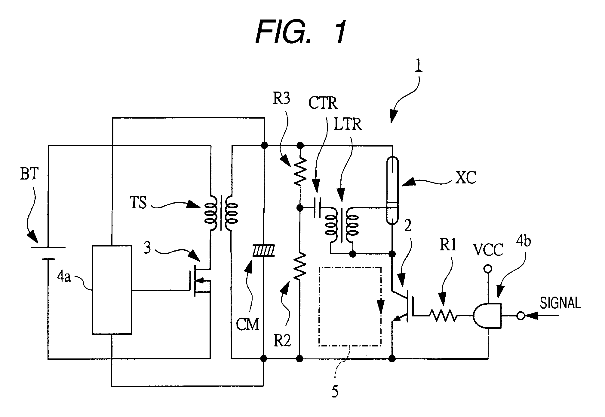
[0110]FIG. 1 is a circuit diagram illustrating an example of the basic circuitry of a flash (strobe) as a light emitting device used in photography and the like.

[0111]The light emitting device (flash, strobe) 1 illustrated in FIG. 1 includes: a xenon tube (discharge tube, discharge lamp, arc tube) XC as a luminescent discharge tube (discharge lamp); IGBT (Insulated Gate Bipolar Transistor) 2 coupled in series with the xenon tube XC; and a main capacitor (capacitor) CM coupled in parallel with a series circuit of the xenon tube XC and the IGBT 2. The IGBT 2 functions as a switching element for the discharge switch of the xenon tube XC and the main capacitor CM is a capacitor for discharging the xenon tube XC. More specifically, the collector of the IGBT 2 is coupled to one internal electrode of the xenon tube XC; the emitter of the IGBT 2 is coupled to one electrode of the main capacitor CM; and the other electrode of the main capacitor CM is coupled to the other internal elect...

second embodiment

[0219]FIG. 22 is a planar transparent view of a semiconductor device SM1a in a second embodiment. FIG. 22 corresponds to FIG. 11 and shows an overall plan view illustrating the interior of the package PA seen through. FIG. 23 is a planar transparent view of the semiconductor device SM1a in FIG. 22 with the metal plate MPL, wires BW, and semiconductor chips CP1, CP2, CP3 further removed (seen through) and corresponds to FIG. 13. Though FIG. 23 is a plan view, in FIG. 23, a die pad DP4, lead wirings LDA, LDA1, and leads LD are hatched with oblique lines and the material (resin material) comprising the package PA is hatched with dots to facilitate visualization. FIG. 24 and FIG. 25 are sectional views (lateral sectional view) of the semiconductor device SM1a and are respectively taken in substantially the same sectional positions as in FIG. 6 and FIG. 9. FIG. 24 substantially corresponds to a sectional view of the semiconductor device SM1a taken in the position of line A-A of FIG. 22; ...

third embodiment

[0230]FIG. 27 is a planar transparent view of a semiconductor device SM1b in a third embodiment. FIG. 27 corresponds to FIG. 11 and shows an overall plan view illustrating the interior of the package PA seen through. FIG. 28 is a planar transparent view of the semiconductor device SM1b in FIG. 27 with the metal plate MPL, wires BW, and semiconductor chips CP1, CP2, CP3 further removed (seen through) and corresponds to FIG. 13. Though FIG. 28 is a plan view, in FIG. 28, a die pad DP1, DP5, lead wiring LDA, and leads LD are hatched with oblique lines and the material (resin material) comprising the package PA is hatched with dots to facilitate visualization. FIG. 29 is a sectional view (lateral sectional view) of the semiconductor device SM1b and is taken in substantially the same sectional position as in FIG. 9. FIG. 29 is substantially corresponds to a sectional view of the semiconductor device SM1b taken in the position of line D1-D1 of FIG. 27. A top view and a bottom view of the ...


PUM


Abstract

The size of a light emitting device is reduced. The light emitting device for flash photography includes: a luminescent xenon tube; IGBT for the discharge switch of the xenon tube; a capacitor for discharging the xenon tube; and MOSFET for the charge switch of the capacitor. A semiconductor device used in this light emitting device is obtained by sealing the following in a package: a semiconductor chip in which the IGBT is formed; a semiconductor chip in which the MOSFET is formed; a semiconductor chip in which a drive circuit of the IGBT and a control circuit of the MOSFET are formed; and multiple leads coupled thereto.

Description

CROSS-REFERENCE TO RELATED APPLICATIONS[0001]The disclosure of Japanese Patent Application No. 2009-95084 filed on Apr. 9, 2009 including the specification, drawings and abstract is incorporated herein by reference in its entirety.BACKGROUND OF THE INVENTION[0002]The present invention relates to semiconductor devices and in particular to a technology effectively applicable to semiconductor devices used in light emitting devices for flash photography.[0003]In recent years, the numbers of pixels of cameras built in cellular phones have been more and more increased and cellular phones equipped with a megapixel camera are becoming widely used. In these circumstances, the light emitting devices for flash photography of cameras built in cellular phones have increasingly adopted a xenon tube large in quantity of light, not a conventional LED.[0004]Japanese Unexamined Patent Publication No. 2003-21860 (Patent Document 1) describes a technology related to a strobe unit for cameras.[0005]Japa...

Claims


Application Information

Patent Timeline
IPC IPC(8): H05B37/02H01L27/06
CPCH01L23/49575H01L2924/1305H01L25/165H01L2224/32245H01L2224/48091H01L2224/48137H01L2224/48247H01L2224/73221H01L2224/73265H01L2924/01004H01L2924/01013H01L2924/01029H01L2924/01033H01L2924/01046H01L2924/01078H01L2924/01079H01L2924/01082H01L2924/3011H01L24/34H01L2924/07802H01L2924/1306H01L2924/30107H01L2924/13055H01L2924/13091H01L2924/01074H01L2924/01047H01L2924/01023H01L2924/01006H01L2924/01005H01L24/48H01L2924/00014H01L2924/00H01L2924/181H01L2224/40095H01L2224/40245H01L24/40H01L2224/45144H01L24/45H01L2224/371H01L2224/84801H01L2224/83801H01L2224/8385H01L2224/8485H01L24/37H01L2224/0603H01L2224/49111H01L24/49H01L2224/05554H01L2224/49171H01L2224/06181H01L24/84H01L2924/18301H01L2924/00012H01L2224/45015H01L2924/207
Inventor KAWANO, MAKOTOBITO, KATSUTOSHIMITAMURA, ATSUSHIKAWANO, KOHEI
Owner RENESAS ELECTRONICS CORP
Why Eureka
Try Eureka