Receive circuit for connectors with variable complex impedance

a technology of complex impedance and receiver circuit, which is applied in the field of circuits, can solve the problems of increasing introduce additional packaging and reliability challenges, and increase the difficulty of existing inter-chip connections to provide suitable communication characteristics, etc., and achieve the effect of reducing signal distortion

Active Publication Date: 2010-10-21
ORACLE INT CORP
View PDF3 Cites 31 Cited by
  • Summary
  • Abstract
  • Description
  • Claims
  • Application Information

AI Technical Summary

Benefits of technology

[0010]One embodiment of the present invention provides a semiconductor die that includes a receive connector that is proximate to or on a surface of the semiconductor die. This receive connector mechanically and electrically couples to one or more first inter-component connectors, thereby defining a receive variable complex impedance between the receive connector and the one or more first inter-component connectors. Note that the receive variable complex impedance corresponds to a first resistor in parallel with a first capacitor. Moreover, the semiconductor die includes a receive circuit, which is electrically coupled to the receive connector, that receives an electrical signal. This receive circuit mitigates signal distortion associated with the receive variable complex impedance.
[0019]Another embodiment provides a method for communicating an electrical signal, which may be performed by the semiconductor die (or one or more circuits on the semiconductor die). During operation, the semiconductor die receives the electrical signal from the receive connector that is mechanically and electrically coupled to one or more inter-component connectors. Note that there is a receive variable complex impedance between the receive connector and the one or more inter-component connectors, and this receive variable complex impedance corresponds to the first resistor in parallel with the first capacitor. Then, the semiconductor die characterizes the receive variable complex impedance based at least in part on the received electrical signal. Next, the semiconductor die configures the receive circuit to mitigate signal distortion associated with the receive variable complex impedance based at least in part on the characterization of the receive variable complex impedance.

Problems solved by technology

As integrated-circuit (IC) technology continues to scale to smaller critical dimensions, it is increasingly difficult for existing inter-chip connections to provide suitable communication characteristics, such as: high bandwidth, low power, reliability and low cost.
However, the proposed techniques often introduce additional packaging and reliability challenges.
It can be difficult to maintain this alignment in the presence of vibrations and thermal stress using a low-cost chip package.
Furthermore, the capacitance of the inter-chip contacts can be small, which makes it challenging to couple high-capacity power supplies using PxC.
However, microsprings are typically required to make and maintain conductive contacts with connectors on ICs.
In order to achieve such conductive contacts, the microsprings typically have sharp tips that can scrape through any oxide or passivation layers above the connectors on the ICs during a scrub-in process, which increases the fabrication costs of the microsprings.
Furthermore, conductive contacts are often achieved by increasing the force between the microsprings and the connectors on an IC in a chip package, which also increases cost.
In addition, the sharp tips and large forces can produce foreign particles (such as debris) that can reduce the conductivity of contacts over time, thereby reducing reliability and limiting the number of mating cycles.
Similar to microsprings, anisotropic films often suffer from reliability issues due to the potential for the conductive elements to fail to make adequate contact with each other and with the chip pad.
In general, higher forces within a chip package decrease the chip-package reliability in other ways and increase the packaging cost.
However, this approach introduces additional challenges.
For example, the capacitive (or inductive) signaling techniques used in PxC typically do not tolerate conductive inter-chip contacts.
This thicker oxide layer reduces the energy that is capacitively coupled between chips, which makes receiving electrical signals more difficult.
In addition, it limits the amount of power that can be supplied to an IC via capacitively coupled microsprings or anisotropic films.

Method used


Image

  • Receive circuit for connectors with variable complex impedance
  • Receive circuit for connectors with variable complex impedance
  • Receive circuit for connectors with variable complex impedance

Examples


Embodiment Construction

[0039]The following description is presented to enable any person skilled in the art to make and use the invention, and is provided in the context of a particular application and its requirements. Various modifications to the disclosed embodiments will be readily apparent to those skilled in the art, and the general principles defined herein may be applied to other embodiments and applications without departing from the spirit and scope of the present invention. Thus, the present invention is not intended to be limited to the embodiments shown, but is to be accorded the widest scope consistent with the principles and features disclosed herein.

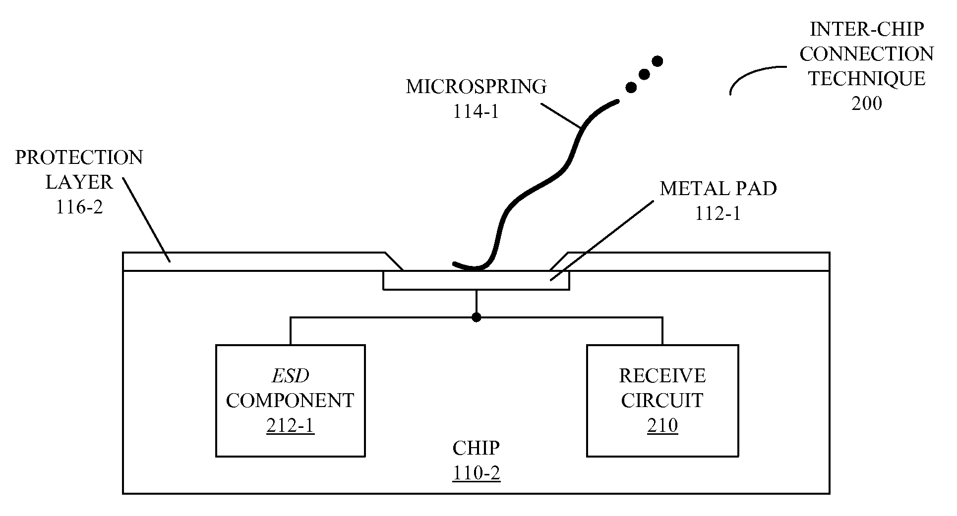
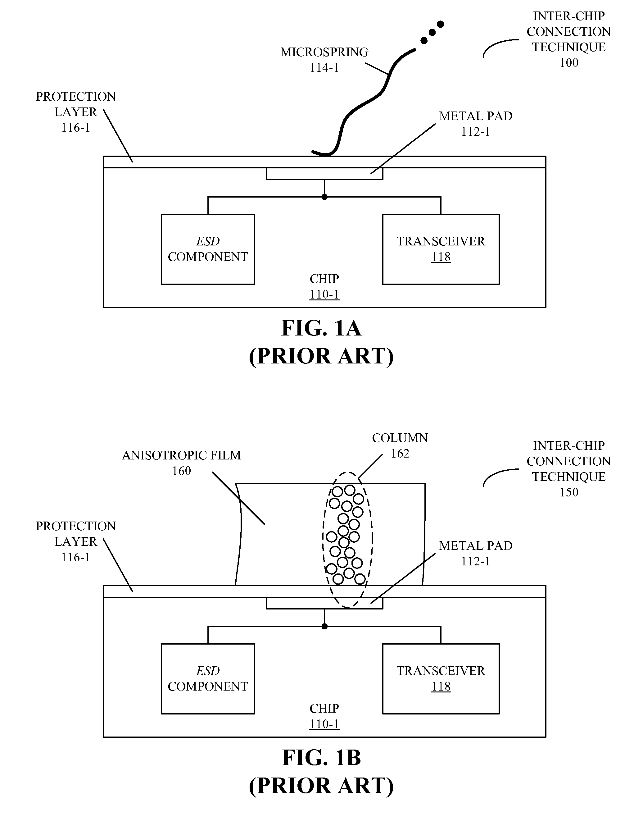
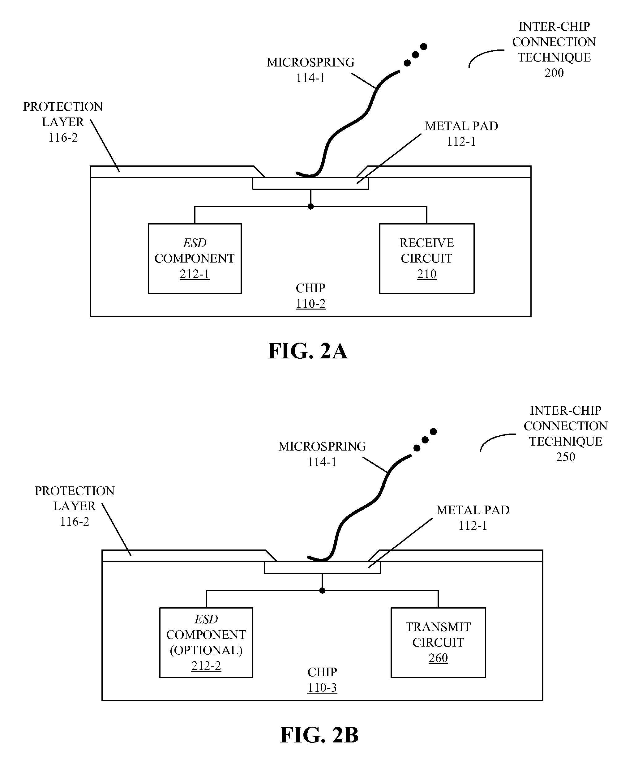
[0040]Embodiments of a circuit for use with an inter-chip connection that has a variable complex impedance (which can be conductive, capacitive or both), a system that includes the circuit, and a communication technique are described. This inter-chip connection may be formed between a microspring or an anisotropic film and a metal connector on ...


PUM


Abstract

Embodiments of a circuit for use with an inter-chip connection that has a variable complex impedance (which can be conductive, capacitive or both), a system that includes the circuit, and a communication technique are described. This inter-chip connection may be formed between a microspring or an anisotropic film and a metal connector on or proximate to a surface of a chip. Moreover, the circuit may mitigate signal distortion associated with the variable complex impedance. For example, the circuit may include an internal impedance that is electrically coupled in series with the metal connector, and that has an impedance which dominates the variable complex impedance over a range of operating frequencies. Separately or additionally, the circuit may be adapted to correct for the signal distortion.

Description

BACKGROUND[0001]1. Field of the Invention[0002]The present invention relates to circuits that mitigate signal distortion caused by a variable complex impedance between a connector on a semiconductor die and one or more microspring or anisotropic-film inter-component connectors.[0003]2. Related Art[0004]As integrated-circuit (IC) technology continues to scale to smaller critical dimensions, it is increasingly difficult for existing inter-chip connections to provide suitable communication characteristics, such as: high bandwidth, low power, reliability and low cost. Several technologies have been proposed to address this problem. These proposed technologies include: proximity communication or PxC (for example, with capacitive inter-chip contacts), inter-chip microsprings (with conductive inter-chip contacts), anisotropic films (for example, where the anisotropic film includes an elastomer), and a combination of PxC with microsprings (with capacitive inter-chip contacts). However, the ...

Claims


Application Information

Patent Timeline
Patent Type & Authority Applications(United States)
IPC IPC(8): H03K19/003
CPCH01L23/3171H01L2224/02166H01L23/5223H01L23/5225H01L23/552H01L23/585H01L23/60H01L23/642H01L23/645H01L23/647H01L23/66H01L24/05H01L24/06H01L24/13H01L24/72H01L24/90H01L25/0655H01L25/0657H01L25/50H01L27/0251H01L2223/6622H01L2223/6627H01L2223/6655H01L2224/05556H01L2224/05624H01L2224/13099H01L2224/95145H01L2225/06527H01L2924/01013H01L2924/01033H01L2924/01074H01L2924/014H01L2924/15311H01L2924/15312H01L2924/19033H01L2924/19041H01L2924/19042H01L2924/19043H01L2924/19051H01L2924/30105H01L2924/3011H01L2924/3025H03H7/38H01L23/48H01L2924/12032H01L2224/0401H01L2924/01023H01L2924/01019H01L2924/01006H01L2924/00014H01L2924/00H01L2924/351H01L2924/14H01L2224/32145H01L2224/83851H01L2224/29291
Inventor DROST, ROBERT J.HOPKINS, ROBERT D.CHOW, ALEX
Owner ORACLE INT CORP
Why Eureka
Try Eureka