Manufacturing method of semiconductor device

Active Publication Date: 2010-10-21
RENESAS ELECTRONICS CORP
View PDF6 Cites 16 Cited by
  • Summary
  • Abstract
  • Description
  • Claims
  • Application Information

AI Technical Summary

Benefits of technology

[0038]Further, in the present application, when it is referred to as “semiconductor device”, this means a device comprising primarily various kinds of transistors (active elements), and resistors, capacitors, etc. integrated, for example, over a semiconductor chip, etc. (f

Problems solved by technology

However, according to the study made by the present inventors, it has been foun

Method used


Image

  • Manufacturing method of semiconductor device
  • Manufacturing method of semiconductor device
  • Manufacturing method of semiconductor device

Examples


Embodiment Construction

Summary of the Preferred Embodiments

[0036]At first, the outline for typical embodiments of the invention disclosed in the present application is to be described.

1. A manufacturing method of a semiconductor device includes the steps of:

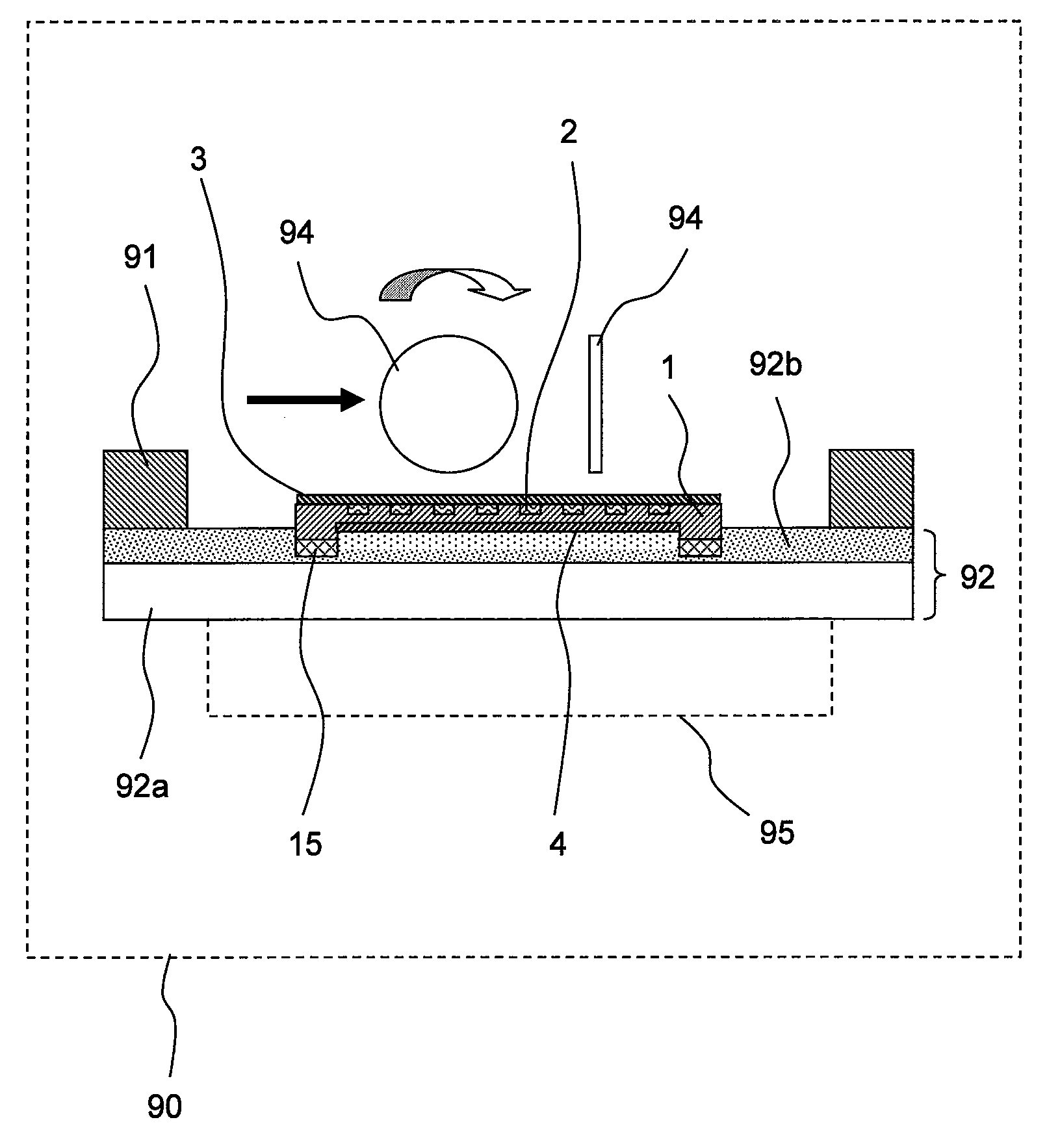
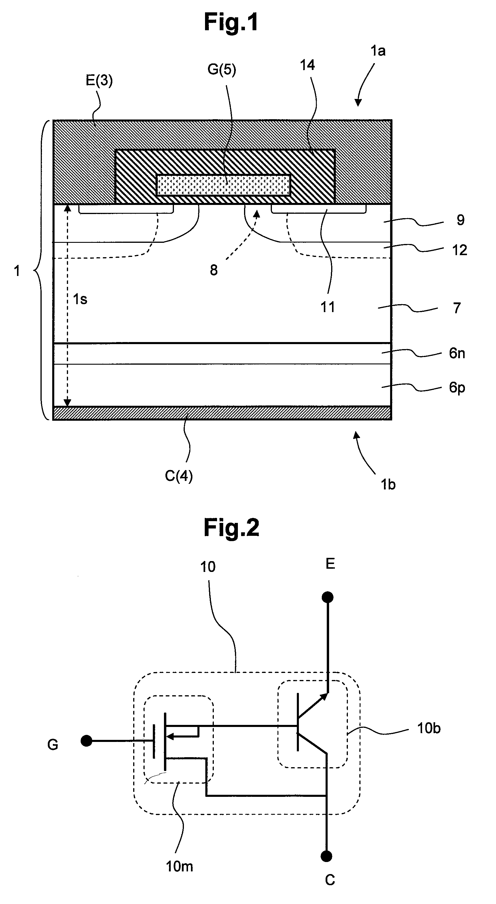
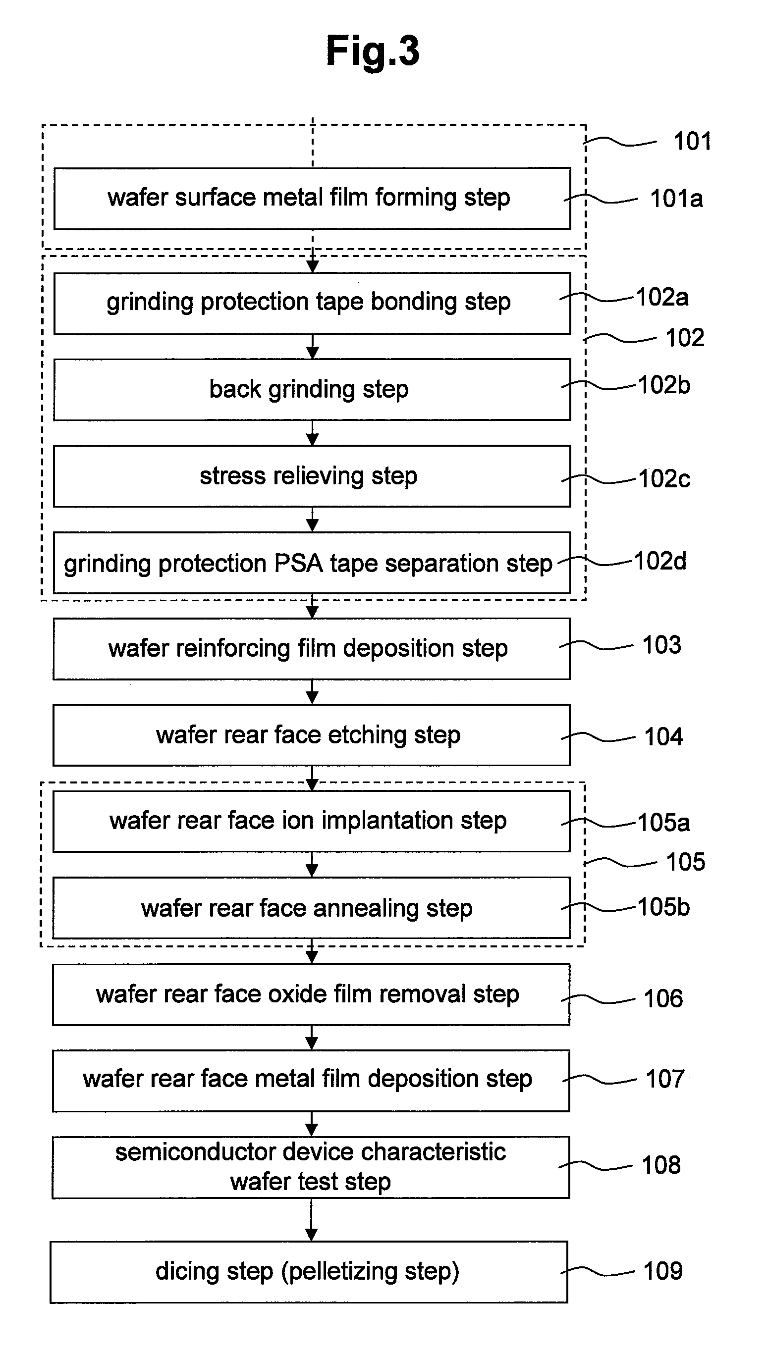
(a) forming a first metal film over a first main surface of a semiconductor wafer having a first thickness;

(b) conducting, after the step (a), back grinding to a second main surface of the semiconductor wafer thereby making a second thickness thinner than the first thickness;

(c) forming, after the step (b), an insulation film pattern comprising a first insulation film and containing an annular insulation film pattern along the periphery of a second main surface of the semiconductor wafer over the second main surface along the periphery thereof;

(d) making the thickness for the opening of the annular insulation film pattern to a third thickness which is thinner than the second thickness in a state where the insulation film pattern is present;

(e) conducti...


PUM


Abstract

In a process for a semiconductor typically represented by a vertical power MOSFET, etc. of repeating various fabrications in a state of a thin film wafer with the thickness of the wafer being 200 μm or less, it is a standard procedure of conducting processing in a stage of bonding a reinforcing glass sheet to a device surface of the wafer (main surface on the side of surface) in the step after film thickness-reduction. However according to the study of the present inventors, it has been found that about 70% for the manufacturing cost is concerned with the reinforcing glass sheet. In the present invention, a stress relief insulation film pattern is formed to the peripheral end of the rear face of a wafer in which processing to the device surface (surface side face) of the wafer has been completed substantially and back grinding has been applied.

Description

CLAIM OF PRIORITY[0001]The present application claims priority from Japanese patent application JP2009-101679 filed on Apr. 20, 2009, the content of which is hereby incorporated by reference into this application.FIELD OF THE INVENTION[0002]The present invention concerns a technique which is applied effectively to a wafer handling technique in a manufacturing method of a semiconductor device (or a semiconductor integrated circuit device).BACKGROUND OF THE INVENTION[0003]Patent Document 1 describes a technique of appending a seal member to the periphery of a wafer thereby leaving a thick peripheral portion as it is for preventing cracking or bending of the wafer upon etching the wafer rear face for lowering the on resistance of a vertical type MOSFET (Metal Oxide Semiconductor Field Effect Transistor).[0004]Patent Document 2 describes a technique for improving the strength and the durability of the wafer in a vertical power device by forming a rim-shaped hard mask with a silicon nitr...

Claims


Application Information

Patent Timeline
IPC IPC(8): H01L21/66H01L21/78
CPCH01L21/3083H01L21/6835H01L21/78H01L22/14H01L29/66333H01L29/7395H01L2221/6834H01L2924/0002H01L2924/13055H01L2924/13091H01L2924/19041H01L2924/00
Inventor AMADA, HARUOSHIMAZAWA, KENJI
Owner RENESAS ELECTRONICS CORP
Why Eureka
Try Eureka