Organic el element and organic el material-containing solution
a technology of organic el and organic el, which is applied in the field of organic el devices, can solve the problems of difficult to adopt such a structure, difficult to achieve blue to green emission, and complicated manufacturing process, and achieves the effects of improving efficiency, reducing cost, and increasing device li
- Summary
- Abstract
- Description
- Claims
- Application Information
AI Technical Summary
Benefits of technology
Problems solved by technology
Method used
Image
Examples
example 1
[0386]A glass substrate (size: 25 mm×75 mm×1.1 mm thick) having an ITO transparent electrode (manufactured by Geomatec Co., Ltd.) was ultrasonic-cleaned in isopropyl alcohol for five minutes, and then UV / ozone-cleaned for 30 minutes.
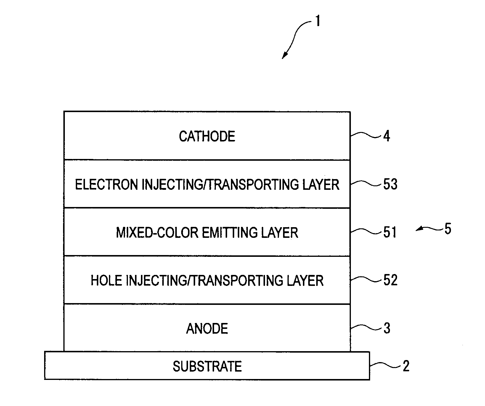
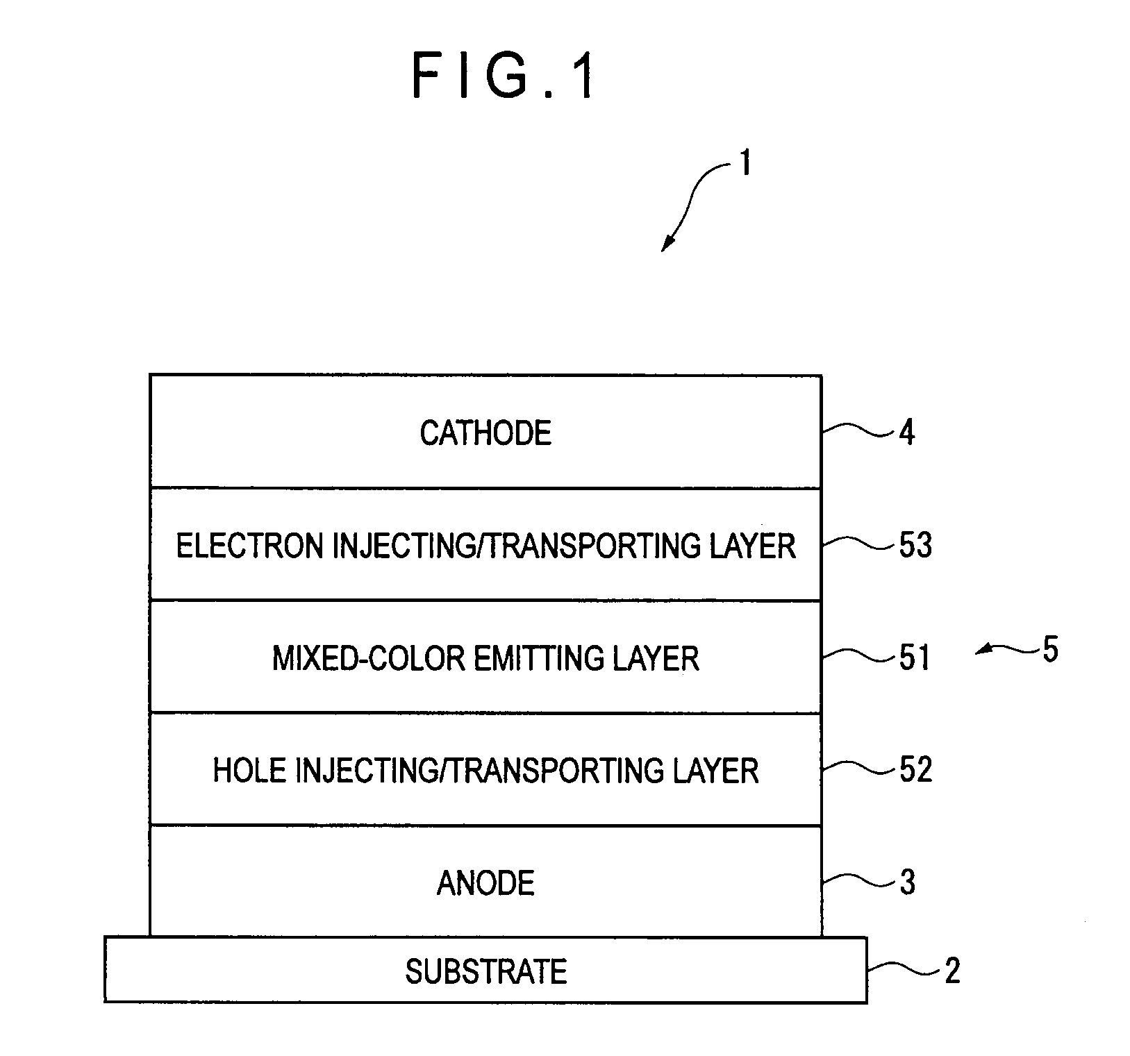
[0387]After the glass substrate having the transparent electrode line was cleaned, the glass substrate was mounted on a substrate holder of a vacuum deposition apparatus. Then, 55-nm thick film of 4,4′-bis[N-(1-naphthyl)-N-phenylamino]biphenyl (hereinafter abbreviated as “NPD film”) was initially formed by resistance heating deposition onto a surface of the glass substrate where the transparent electrode line was provided so that the NPD film covered the transparent electrode. The NPD film served as the hole injecting / transporting layer.
[0388]A 40-nm thick film of a compound represented by the following formula (H1) was formed on the NPD film by resistance heating deposition. At the same time, NPD and a compound represented by the following formula (RD) ...
example 2
[0392]An organic EL device was manufactured in the same manner as Example 1, except that the following compound (GD) was deposited as a green fluorescent dopant in addition to the fluorescent dopant and the red phosphorescent dopant so that the compound (GD) was contained at a content of 0.5% (mass ratio) of the compound (H1).
example 3
[0393]An organic EL device was manufactured in the same manner as Example 1, except that a 10-nm-thick green phosphorescent-emitting layer was provided between the mixed-color emitting layer and the hole blocking layer. The green phosphorescent-emitting layer was deposited so that Ir(ppy)3 for green phosphorescent emission was contained at a content of 5% of the CBP (i.e., host).
PUM
 Abstract
Description
Claims
Application Information


