

Optical semiconductor package sealing resin material
- Summary
- Abstract
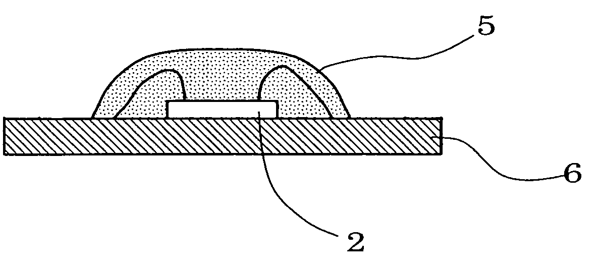
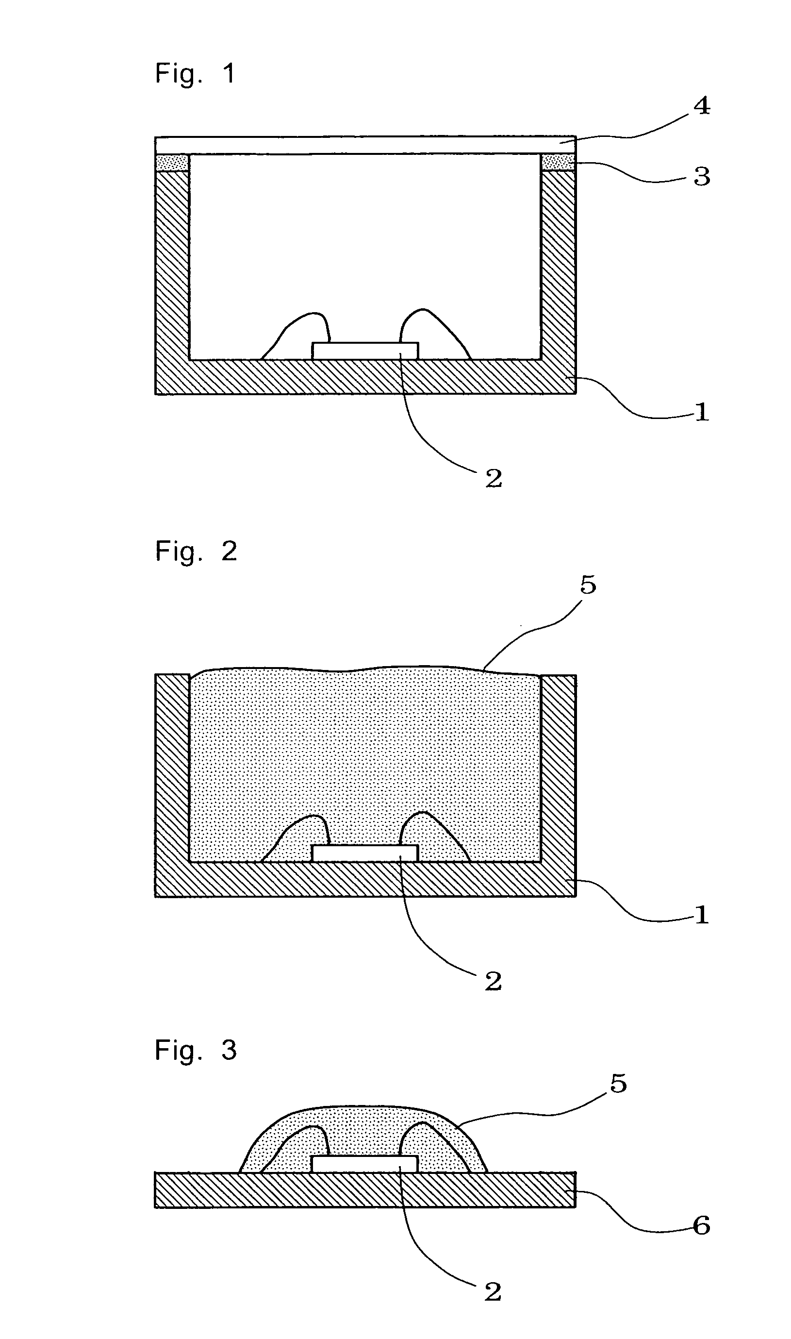
- Description
- Claims
- Application Information
AI Technical Summary
Benefits of technology
Problems solved by technology
Method used
Image

Examples
reference example 1
Preparation of Epoxy-Clay Mineral Dispersion Using Hydrophobic Hectorite
[0040]5 g of hectorite being synthetic smectite (Lucentite SEN, CO-OP CHEMICAL CO., LTD.) was added to 100 g of toluene, and the mixture was stirred at room temperature for 6 hours to disperse the hectorite therein, whereby a viscous clay mineral dispersion was obtained. The chemical formula of the hectorite is represented by Na0.33(Mg2.67Li0.33)Si4O10(OH)2, and polyoxyethylene and alkyl methyl ammonium ions are intercalated between the layers of the hydrophobic hectorite used.
[0041]The obtained clay mineral dispersion was added to an epoxy dispersion prepared in advance by dispersing 45 g of a liquid hydrogenated bisphenol-A epoxy compound (YX8000, Japan Epoxy Resin Co., Ltd.) in 100 g of dimethylformamide, and the mixture was stirred at room temperature for 24 hours to give a colorless transparent epoxy dispersion.
[0042]The obtained epoxy dispersion was concentrated under reduced pressure in an evaporator to g...
reference example 2
Preparation of Epoxy-Clay Mineral Dispersion Using Hydrophobic Bentonite
[0043]5 g of bentonite being synthetic smectite (S-BEN NX, HOJUN Co., Ltd.) was added to 100 g of toluene, and the mixture was stirred at room temperature for 6 hours to disperse the bentonite therein, whereby a viscous clay mineral dispersion was obtained. The chemical formula of the bentonite is generally represented by Na0 to 0.66Ca0 to 0.66(Mg0 to 0.66Al3.34)Si8O20(OH)4 which varies depending on the synthetic conditions, and trioctylammonium ions are intercalated between the layers of the hydrophobic bentonite used.
[0044]The obtained clay mineral dispersion was added to an epoxy dispersion prepared in advance by dispersing 45 g of a liquid hydrogenated bisphenol-A epoxy compound (YX8000, Japan Epoxy Resin Co., Ltd.) in 100 g of toluene, and the mixture was stirred at room temperature for 24 hours to give a colorless transparent epoxy dispersion.
[0045]The obtained epoxy dispersion was concentrated under reduc...
reference example 3
Preparation of Epoxy-Clay Mineral Dispersion Using Hydrophilic Hectorite
[0046]1 g of hectorite being synthetic smectite (Lucentite SEN, CO-OP CHEMICAL CO., LTD.) was added to 99 g of ultrapure water, and the mixture was stirred at room temperature for 6 hours to disperse the hectorite therein, whereby a viscous clay mineral dispersion was obtained. The chemical formula of the hectorite is represented by Na0.33(Mg2.67Li0.33)Si4O10(OH)2, and Na ions and water molecules are intercalated between the layers of the hydrophilic hectorite used.
[0047]An ethanol dispersion of 1 g of tetradecyl ammonium bromide in 7 g of ethanol was added dropwise to the obtained clay mineral dispersion at room temperature and a rate of 0.5 mL / sec under stirring. The mixture was further stirred at room temperature for 6 hours. Then the resultant mixture was filtrated through a 65 μm-mesh filter under reduced pressure, and the hydrophobic clay mineral remaining on the filter was dried at 100° C. for 1 hour. The...
PUM
| Property | Measurement | Unit |
|---|---|---|
| Percent by mass | aaaaa | aaaaa |
| Percent by mass | aaaaa | aaaaa |
| Percent by mass | aaaaa | aaaaa |
Abstract
Description
Claims
Application Information