Nonvolatile latch circuit
a latch circuit and non-volatile technology, applied in the field of non-volatile latch circuits, can solve the problems of increasing operating power, data and processed data potentially disappearing, and complicating power control, so as to reduce the magnetization reversal current
- Summary
- Abstract
- Description
- Claims
- Application Information
AI Technical Summary
Benefits of technology
Problems solved by technology
Method used
Image
Examples
first embodiment
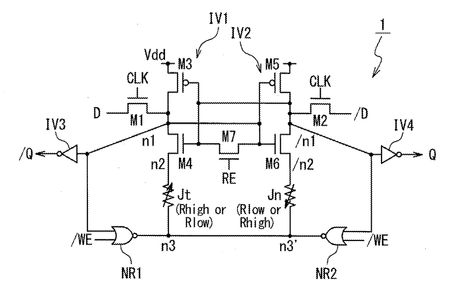
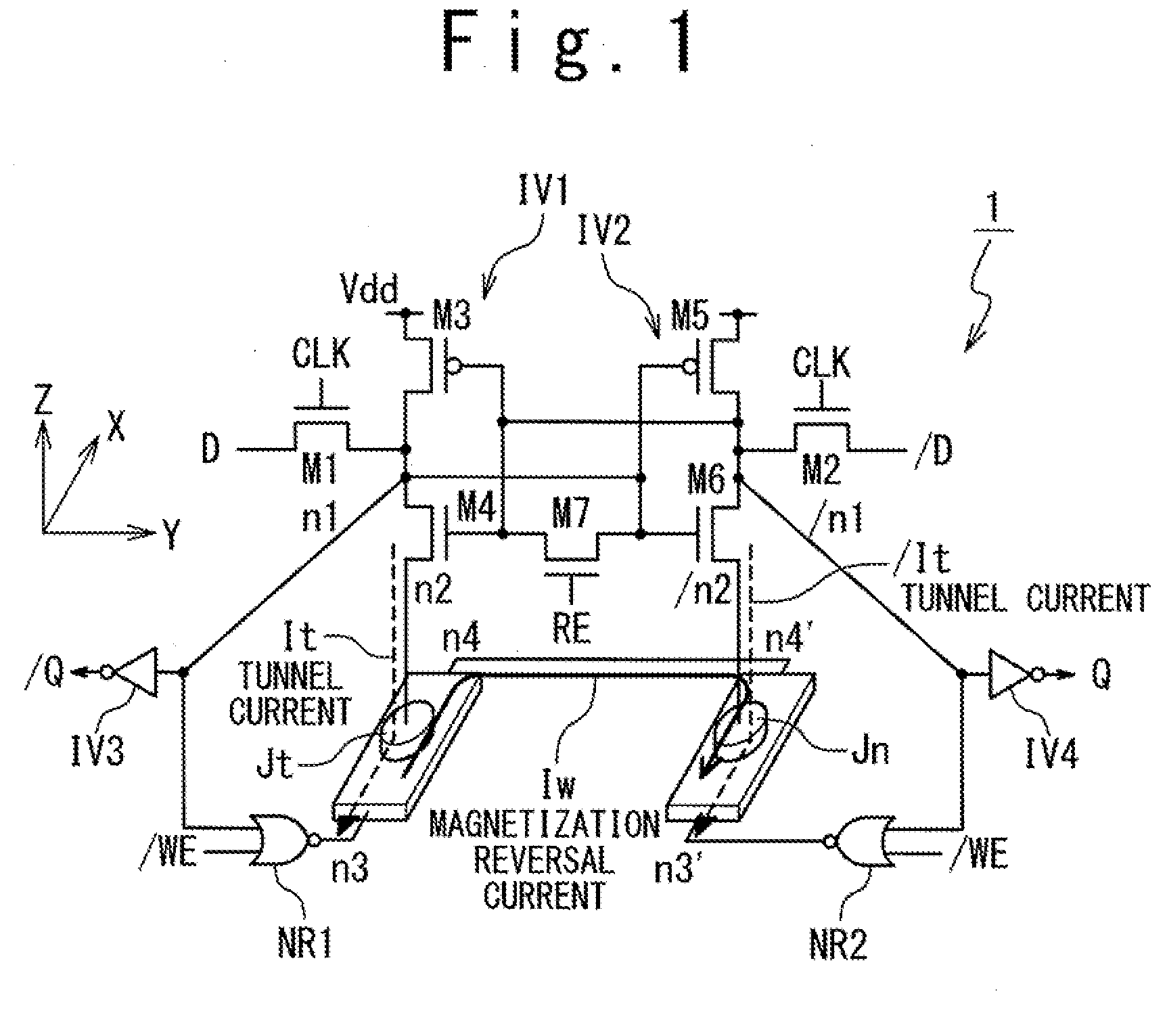
[0025]FIG. 1 is a basic configuration view illustrating a nonvolatile latch circuit 1 in a first embodiment of the present invention. The nonvolatile latch circuit 1 includes two MTJ elements Jt, Jn, NMOS transistors M1, M2, M4, M6, M7, PMOS transistors M3, M5, NOR gates NR1, NR2 and inverters IV3, IV4.
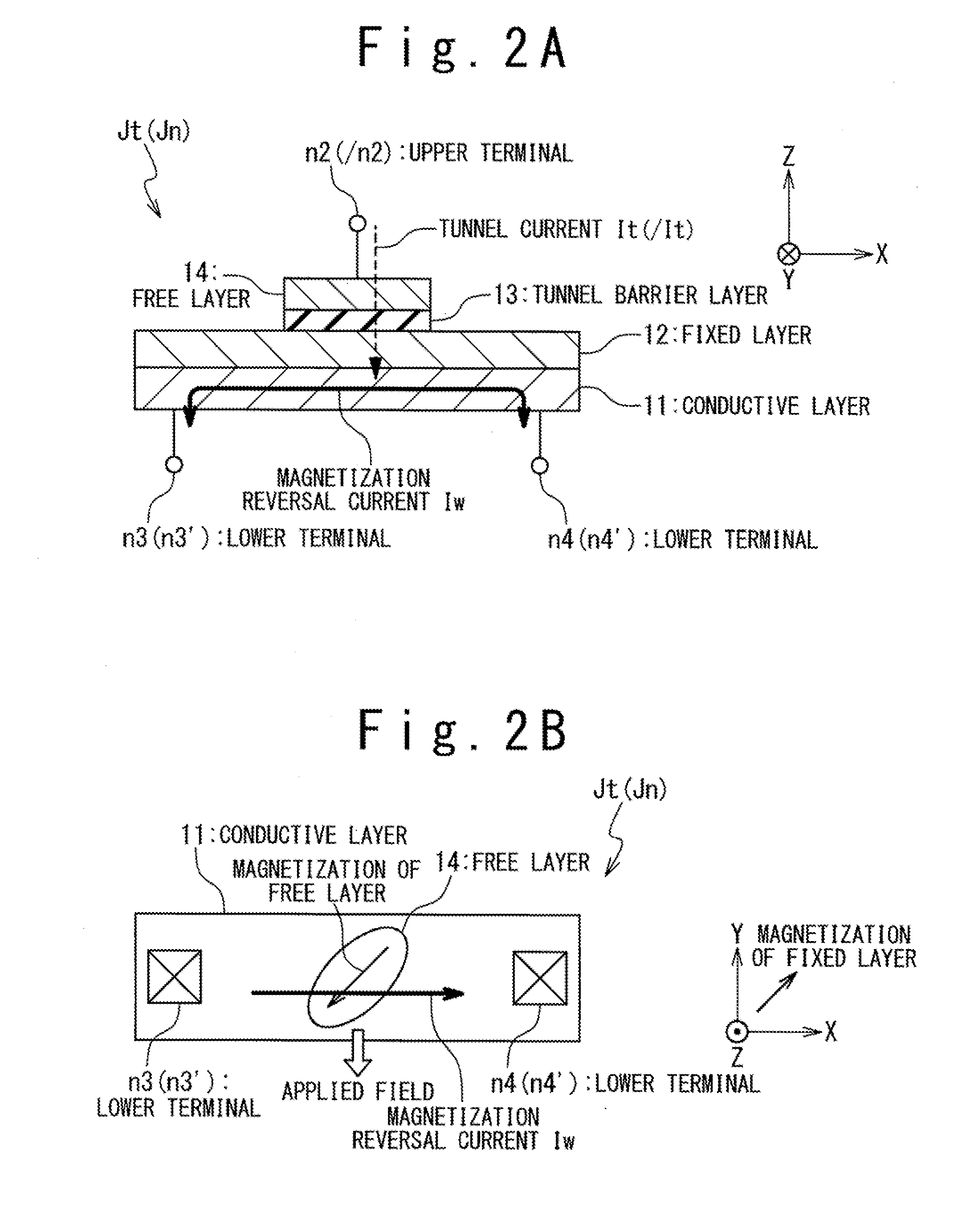
[0026]The MTJ elements Jt and Jn are used to store data in the nonvolatile latch circuit 1 when power is not supplied to the nonvolatile latch circuit 1. In this embodiment, the MTJ elements Jt and Jn are configured as a three terminal element. Specifically, the MTJ element Jt includes an upper terminal n2 and two lower terminals n3, n4, and the MTJ element Jn includes an upper terminal / n2 and two lower terminals n3′, n4′. The lower terminals n4 and n4′ of the MTJ elements Jt and Jn are connected to each other through an interconnection. As described later, a tunnel current It passing through the MTJ formed within the MTJ element Jt flows from the upper terminal n2 to the lower termi...
second embodiment
[0053]In a second embodiment of the present invention, a nonvolatile latch circuit of the present invention is configured so as to operate as a delay flipflop (D-FF). A nonvolatile D flipflop circuit 1C in the second embodiment has a configuration in which a commonly-used master-slave typed D-FF is modified to use the high-through nonvolatile latch circuit 1 shown in FIG. 4 as a slave latch.
[0054]In detail, the nonvolatile D flipflop circuit 1C in the second embodiment includes a master latch 31, a slave latch 32 and inverters IV22 to IV24. The master latch 31 includes clocked inverters CI1, CI2 and an inverter IV21.
[0055]The clocked inverter CI1 includes PMOS transistors M21, M22, NMOS transistors M23 and M24. The input data D are supplied to the gates of the PMOS transistor M21 and the NMOS transistor M24. A non-inverted signal p1 of the clock signal CLK is inputted to the gate of the PMOS transistor M22 and the inverted signal / p1 of the clock signal CLK is inputted to the gate o...
PUM
 Abstract
Description
Claims
Application Information


