Mocvd single chamber split process for LED manufacturing

a single-chamber split and led manufacturing technology, applied in the field of manufacturing devices, can solve problems such as process conditions drift, affecting and achieve the effect of improving process reproducibility and uniformity

Inactive Publication Date: 2010-10-28
APPLIED MATERIALS INC
View PDF77 Cites 111 Cited by
  • Summary
  • Abstract
  • Description
  • Claims
  • Application Information

AI Technical Summary

Benefits of technology

[0009]Embodiments described herein generally relate to methods for forming Group III-V materials by metal-organic chemical vapor deposition (MOCVD) processes. In one embodiment, a method for fabricating a compound nitride semiconductor structure is provided. The method comprises depositing a first layer over one or more substrates with a thermal chemical-vapor-deposition process within a processing chamber using a first group-III precursor comprising a first group-III element and a first nitrogen containing precursor, wherein the first layer comprises nitrogen and the first group-III element, removing the one or more substrates from the processing chamber after depositing a first layer without exposing the one or more substrates to atmosphere, flowing a first cleaning gas into the processing chamber to remove contaminants from the processing chamber after removing the one or more substrates from the processing chamber after depositing a first layer, transferring the one or more substrates into the processing chamber without exposing the one or more substrates to atmosphere after removing contaminants from the processing chamber; and depositing a second layer over the first layer with a thermal chemical-vapor-deposition process within the processing chamber using a second group-III precursor and a second nitrogen containing precursor, wherein the second group-III precursor comprises a second group-III element not comprised by the first group-III precursor.
[0010]In another embodiment, a method for fabricating a compound nitride semiconductor structure is provided. The method comprises positioning one or more substrates on a susceptor in a processing region of a metal organic chemical vapor deposition (MOCVD) chamber comprising a showerhead, depositing a gallium nitride layer over the substrate with a thermal chemical-vapor-deposition process within the MOCVD chamber by flowing a first gallium containing precursor and a first nitrogen containing precursor through the showerhead into the MOCVD chamber, removing the one or more substrates from the MOCVD chamber without exposing the one or more substrates to atmosphere, flowing a chlorine gas into the processing chamber to remove contaminants from the showerhead, transferring the one or more substrates into the MOCVD chamber after removing contaminants from the showerhead; and depositing an InGaN layer over the GaN layer with a thermal chemical-vapor-deposition process within the MOCVD chamber by flowing a second gallium containing precursor, an indium containing precursor, and a second nitrogen containing precursor into the MOCVD chamber.
[0011]In yet another embodiment, an integrated processing system for manufacturing compound nitride semiconductor devices is provided. The integrated processing system comprises a metal organic chemical vapor deposition (MOCVD) operable to form a gallium nitride (GaN) layer over one or more substrates with a thermal chemical-vapor-deposition process and to form a multi-quantum well (MQW) layer over the GaN layer and a halogen containing gas source coupled with the MOCVD chamber operable for flowing a halogen containing gas into the MOCVD chamber to remove at least a portion of unwanted deposition build-up deposited when forming the GaN layer over the one or more substrate from one or more interior surfaces of the MOCVD chamber prior to forming the MQW layer over the GaN layer, wherein the halogen containing gas is selected from the group comprising fluorine, chlorine, bromine, iodine, HI gas, HCl gas, HBr gas, HF gas, NF3, and combinations thereof.

Problems solved by technology

Such unwanted deposition may create particles and flakes within the chamber, resulting in the drift of process conditions and more importantly affecting the process reproducibility and uniformity.

Method used


Image

  • Mocvd single chamber split process for LED manufacturing
  • Mocvd single chamber split process for LED manufacturing
  • Mocvd single chamber split process for LED manufacturing

Examples


example

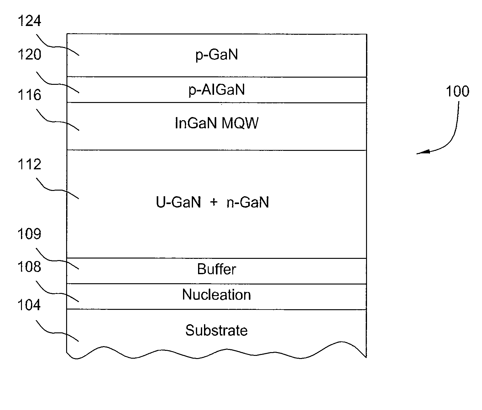
[0051]The following example is provided to illustrate how the general process may be used for the fabrication of compound nitride structures described in connection with processing system 200. The example refers to a LED structure, with its fabrication being performed using a processing system 200 having one MOCVD chamber 202. In one embodiment, the LED structure is similar to structure 100. The cleaning and deposition of the initial GaN layers and deposition of the remaining InGaN, AlGaN, and GaN contact layers may be performed in the MOCVD chamber 202.

[0052]The process begins with a carrier plate 212 containing one or more substrates 340 being transferred into the MOCVD chamber 202. The MOCVD chamber 202 is configured to provide rapid deposition of GaN. A pretreatment process and / or buffer layer is grown over the substrate in the MOCVD chamber 202 using MOCVD precursor gases. This is followed by growth of a thick u-GaN / n-GaN layer, which in this example is performed using MOCVD pr...


PUM

PropertyMeasurementUnit
pressureaaaaaaaaaa
temperatureaaaaaaaaaa

Abstract

In one embodiment a method for fabricating a compound nitride semiconductor device comprising positioning one or more substrates on a susceptor in a processing region of a metal organic chemical vapor deposition (MOCVD) chamber comprising a showerhead, depositing a gallium nitride layer over the substrate with a thermal chemical-vapor-deposition process within the MOCVD chamber by flowing a first gallium containing precursor and a first nitrogen containing precursor through the showerhead into the MOCVD chamber, removing the one or more substrates from the MOCVD chamber without exposing the one or more substrates to atmosphere, flowing a chlorine gas into the processing chamber to remove contaminants from the showerhead, transferring the one or more substrates into the MOCVD chamber after removing contaminants from the showerhead, and depositing an InGaN layer over the GaN layer with a thermal chemical-vapor-deposition process within the MOCVD chamber is provided.

Description

CROSS-REFERENCE TO RELATED APPLICATIONS[0001]This application claims benefit of U.S. provisional patent application Ser. No. 61 / 173,552 (14309L), filed Apr. 28, 2009, which is herein incorporated by reference it its entirety.BACKGROUND OF THE INVENTION[0002]1. Field of the Invention[0003]Embodiments of the present invention generally relate to the manufacturing of devices, such as light emitting diodes (LEDs), laser diodes (LDs) and, more particularly, to processes for forming Group III-V materials by metal-organic chemical vapor deposition (MOCVD) deposition processes.[0004]2. Description of the Related Art[0005]Group III-V films are finding greater importance in the development and fabrication of a variety of semiconductor devices, such as short wavelength LEDs, LDs, and electronic devices including high power, high frequency, high temperature transistors and integrated circuits. For example, short wavelength (e.g., blue / green to ultraviolet) LEDs are fabricated using the Group II...

Claims


Application Information

Patent Timeline
Patent Type & Authority Applications(United States)
IPC IPC(8): H01L51/40H01L21/205
CPCC23C16/303C23C16/4405C23C16/45563H01L33/007H01L21/0237H01L21/0254H01L21/0262C23C16/45574H01L33/02
Inventor KRYLIOUK, OLGA
Owner APPLIED MATERIALS INC
Why Eureka
Try Eureka