Inorganic Nanocrystal Bulk Heterojunctions

a nanocrystal and bulk technology, applied in the field of thin film optoelectronic devices, can solve the problems of high material and manufacturing costs, complex and expensive fabrication processes, and uncompetitive si-based pv power production with conventional fossil fuel-based energy sources, and achieve the effect of low device manufacturing costs

Inactive Publication Date: 2010-11-04
BROOKHAVEN SCI ASSOCS
View PDF10 Cites 43 Cited by
  • Summary
  • Abstract
  • Description
  • Claims
  • Application Information

AI Technical Summary

Problems solved by technology

Despite the continued progression of Si thin film PVs, their material and manufacturing costs remain relatively high, making Si-based PV power production uncompetitive with conventional fossil fuel-based energy sources.
Contributing factors include the need for large Si film thicknesses for efficient light absorption (≧200 μm), as well as their complex and expensive (requiring both time and energy) fabrication processes.
However, planar organic heterojunctions are generally inefficient as a photo-active layer since the diffusion length of generated bound electron-hole pairs (excitons) is much smaller than the optical absorption length.
Despite the potential of organic bulk heterojunction PVs, the highest PCE of these devices is only ˜3% to 5%, a value which, despite the lower manufacturing costs, is still too low for commercial applications.
Despite the improvements in organic PV devices achieved using these approaches, realization of commercially viable devices requires much more significant efficiency gains than what has been realized to date.

Method used


Image

  • Inorganic Nanocrystal Bulk Heterojunctions
  • Inorganic Nanocrystal Bulk Heterojunctions
  • Inorganic Nanocrystal Bulk Heterojunctions

Examples


Embodiment Construction

[0021]In the interest of clarity, in describing the present invention, the following terms and acronyms are defined as provided below.

Acronyms:

[0022]CVD: Chemical Vapor Deposition[0023]ITO: Indium Tin Oxide[0024]FTO: Fluorine Tin Oxide[0025]PCE: Power Conversion Efficiency[0026]PV: Photovoltaic[0027]RIE: Reactive Ion Etching

Definitions

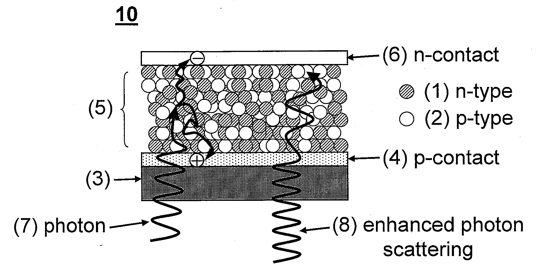
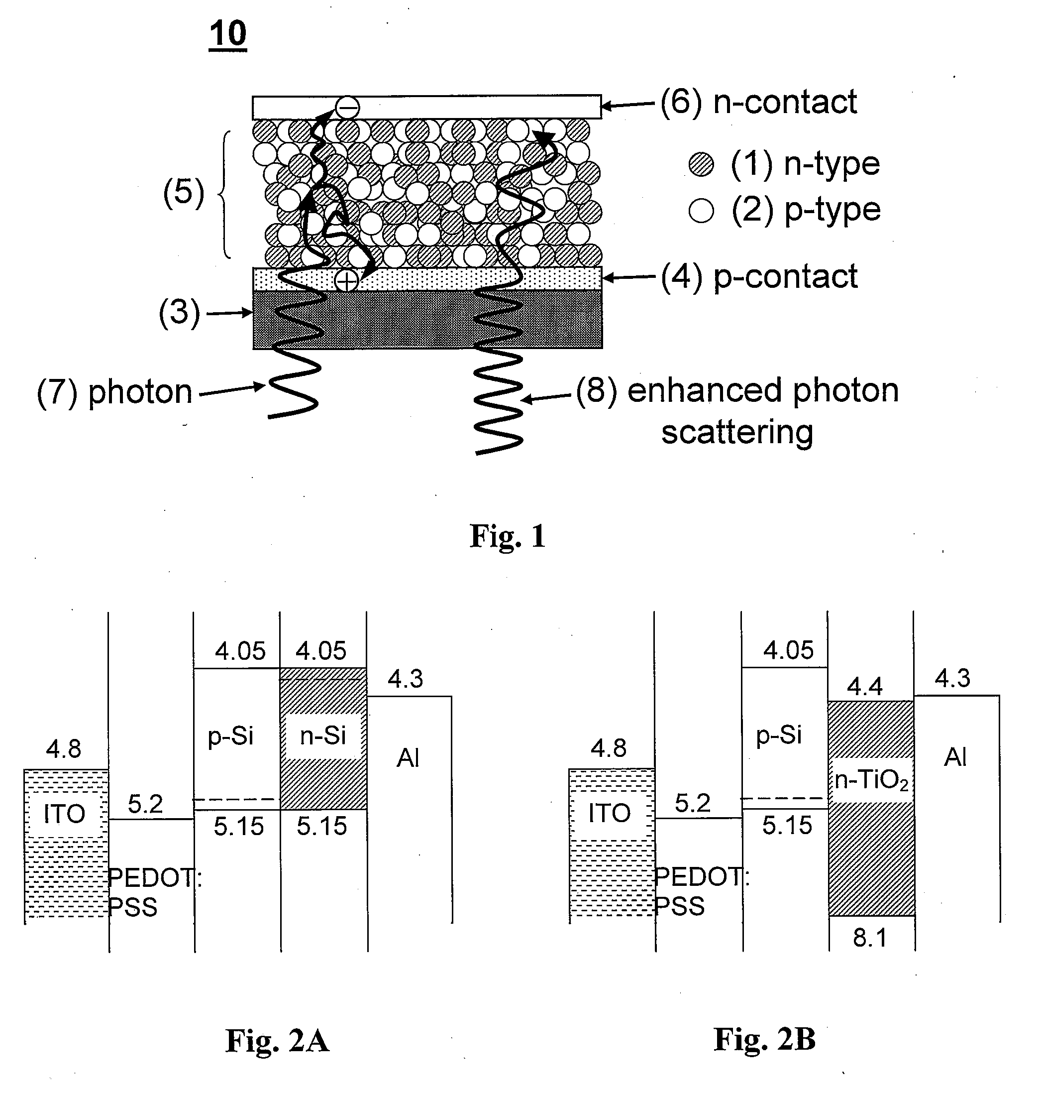
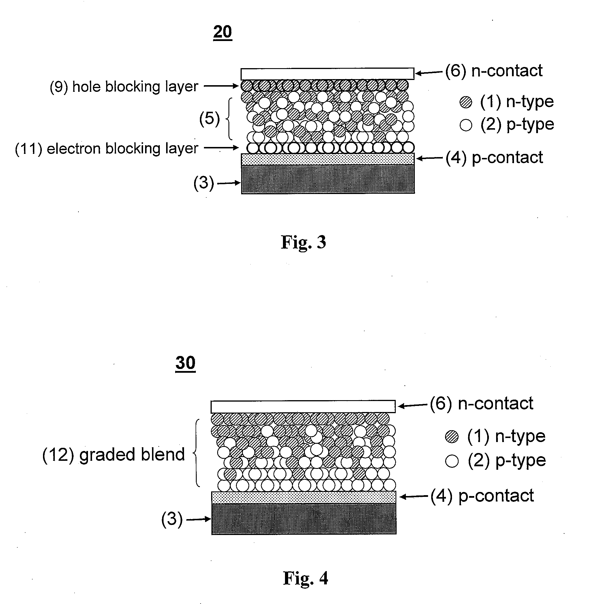
[0028]Acceptor: A dopant atom which, when added to a semiconductor, can form p-type regions.

Donor: A dopant atom which, when added to a semiconductor, can form n-type regions.

Heterojunction: An interface or junction formed between dissimilar materials.

Inorganic: A material or compound which does not contain an organic compound.

Nanocrystal: Any manufactured structure or particle with nanometer-scale dimensions, i.e., 1 to 100 nm.

n-type: A semiconductor for which the predominant charge carriers responsible for electrical conduction are electrons. Normally, donor impurity atoms give rise to the excess electrons.

Optoelectronic: Of or relating to electronic...


PUM

PropertyMeasurementUnit
thicknessaaaaaaaaaa
thicknessaaaaaaaaaa
thicknessaaaaaaaaaa

Abstract

A bulk heterojunction comprising an intermixed blend of fully inorganic n- and p-type particles and its method of manufacture are described. The particles are preferably nanometer-scale, spherical-shaped particles known as nanocrystals which are assembled into a densely packed three-dimensional array. The nanocrystals are preferably fabricated from a photo-active material which, in combination with the nanocrystal shape and size, can be engineered to produce a bulk heterojunction with a specific absorption spectrum. The bulk heterojunction is preferably formed by dispersing a predetermined ratio of the desired n- and p-type nanocrystals in an organic solvent and employing low-cost solution processing techniques to deposit a film having the desired thickness, relative concentration of nanocrystal types, and degree of intermixing onto a substrate. When incorporated as the active layer in optoelectronic devices such solar cells, fully inorganic bulk heterojunctions offer significant improvements in performance while maintaining the low costs associated with organic processing techniques.

Description

[0001]The present invention was made with Government support under Contract No. DE-AC02-98CH10866 awarded by the U.S. Department of Energy. The United States Government has certain rights in the invention.BACKGROUND[0002]I. Field of the Invention[0003]This invention relates generally to thin film optoelectronic devices. In particular, the present invention relates to bulk heterojunctions fabricated with an active layer comprised entirely of inorganic nanocrystals. This invention further relates to the use of inorganic bulk heterojunctions in optoelectronic. devices such as photovoltaic cells.[0004]II. Background of the Related Art[0005]A photovoltaic cell is an energy conversion device capable of converting electromagnetic radiation into electrical energy. When the process involves the conversion of sunlight directly into electricity, this device is commonly referred to as a solar cell. The energy conversion process is based on the photovoltaic (PV) effect in which the absorption of...

Claims


Application Information

Patent Timeline
Patent Type & Authority Applications(United States)
IPC IPC(8): H01L31/0264H01L29/12H01L21/04H01L31/18
CPCH01L21/02521H01L21/02573H01L21/02601H01L21/02628H01L29/165Y02E10/50H01L29/225H01L29/267H01L31/035281H01L31/072H01L33/18H01L29/205
Inventor NAM, CHANG-YONGBLACK, CHARLES T.
Owner BROOKHAVEN SCI ASSOCS
Why Eureka
Try Eureka