Light Emitting Device and Planar Waveguide with Single-Sided Periodically Stacked Interface

a light emitting device and periodic stacking technology, applied in the field of optical device integrated circuit (ic) fabrication, can solve the problems that collimation and alignment cannot always be easily employed, and achieve the effects of improving light collection efficiency, good power budget, and good power budg

Active Publication Date: 2010-11-04
SHARP KK
View PDF7 Cites 0 Cited by
  • Summary
  • Abstract
  • Description
  • Claims
  • Application Information

AI Technical Summary

Benefits of technology

[0012]Disclosed herein is a device with enhanced light collection efficiencies into air for paired Si nano-particle embedded SiOx LEDs and photodetectors, in order to achieve a good power budget for free space optical communications and sensing. Free space optic transmission systems typically require alignment between the light emitted from the light source and the photodetectors to achieve a good power budget, which is necessary for high signal to noise ratios and low bit error rates (BER). However, for simple systems and other design constraints, such collimation and alignments cannot always be easily employed. The device disclosed herein uses a single-sided photonic bandgap (PBG) Bragg reflector to improve the collection efficiency, as compared to conventional SiOx LEDs, making alignment less critical. Also disclosed is a planar waveguide using a PBG Bragg reflector to optimize waveguide coupling.

Problems solved by technology

However, for simple systems and other design constraints, such collimation and alignments cannot always be easily employed.

Method used


Image

  • Light Emitting Device and Planar Waveguide with Single-Sided Periodically Stacked Interface
  • Light Emitting Device and Planar Waveguide with Single-Sided Periodically Stacked Interface
  • Light Emitting Device and Planar Waveguide with Single-Sided Periodically Stacked Interface

Examples


Embodiment Construction

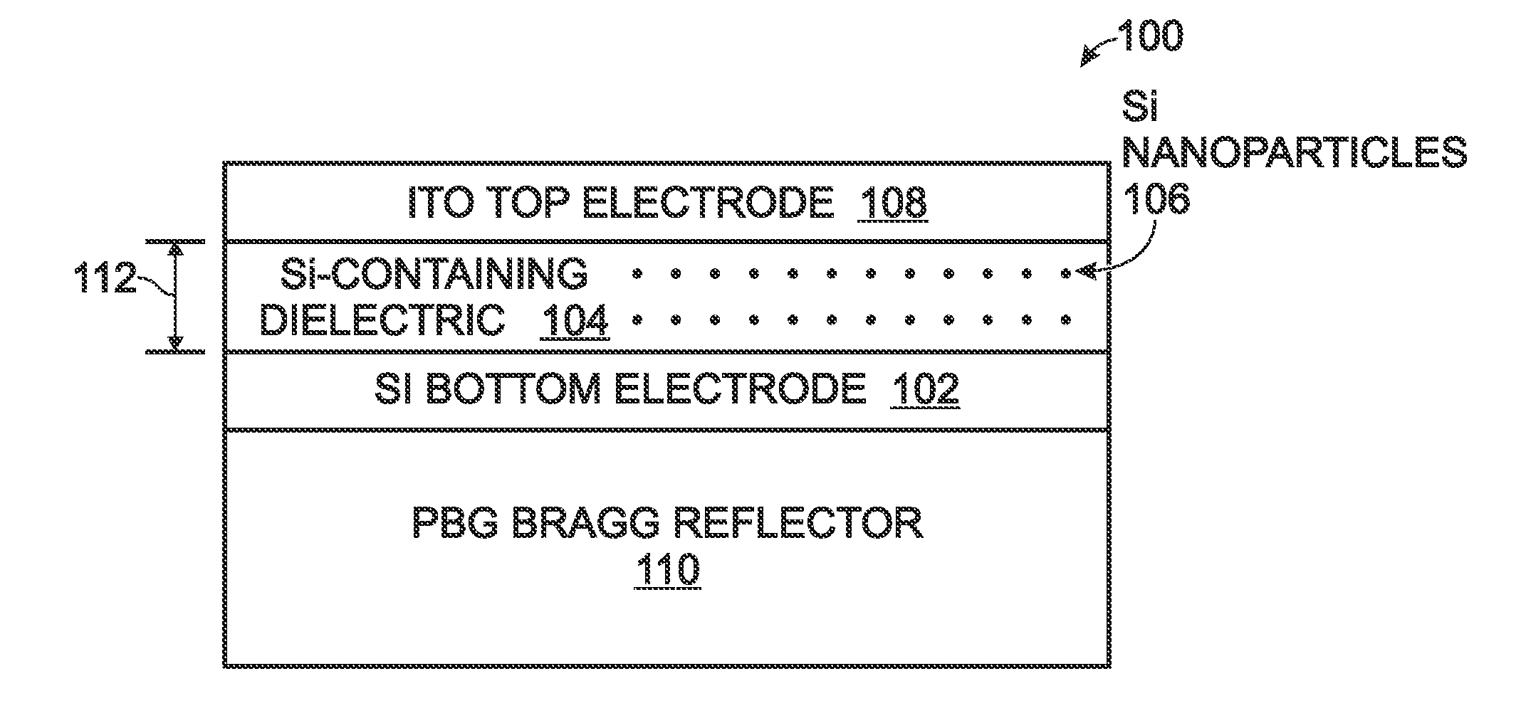
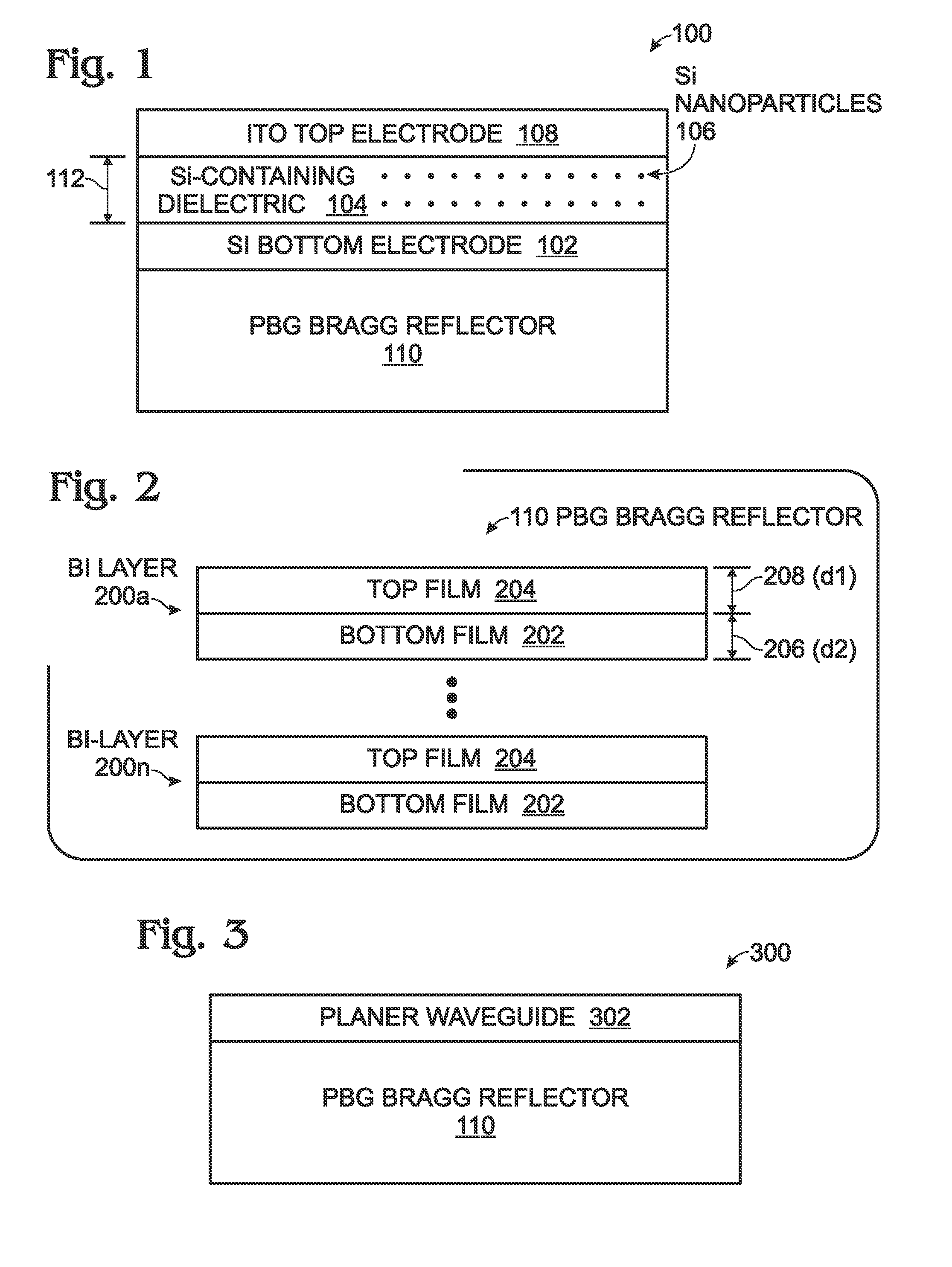
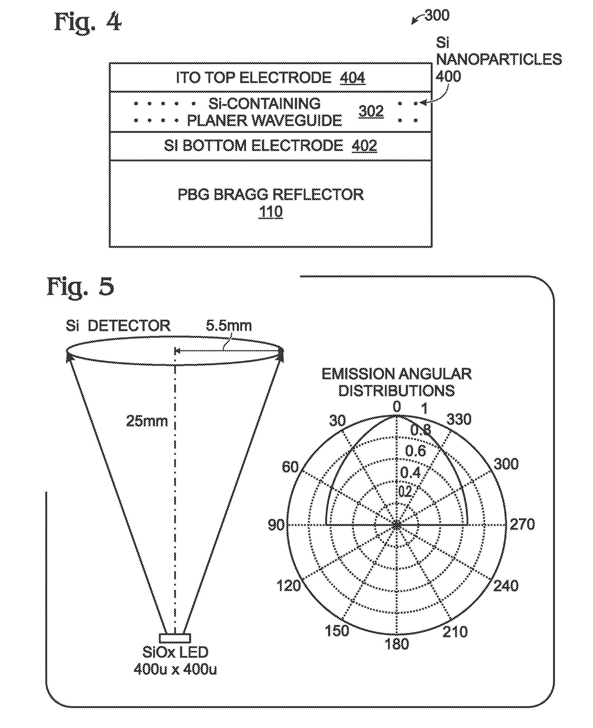
[0032]A distributed Bragg reflector or Bragg reflector is a reflector that may be used in waveguides, such as optical fibers. It is a structure formed from multiple layers of alternating materials with varying refractive indexes, or by periodic variation of some characteristic (such as thickness) of a dielectric waveguide. resulting in periodic variation in the effective refractive index in the guide. Each layer boundary causes a partial reflection of an optical wave. For waves whose wavelength are close to four times the optical thickness of the layers, the many reflections combine with constructive interference, and the layers act as a reflector. The range of wavelengths that are reflected is called the photonic stopband. Within this range of wavelengths, light is “forbidden” to propagate in the structure.

[0033]The reflectivity (R) of a Bragg reflector is given by

R=[no(n2)2N-ns(n1)2Nno(n2)2N+ns(n1)2N]2,

[0034]where ηo, η1, η2 and ηs are the respective refractive indices of the surr...


PUM

PropertyMeasurementUnit
sizeaaaaaaaaaa
thicknessaaaaaaaaaa
refractive indexaaaaaaaaaa

Abstract

Light emitting and waveguide devices with single-sided photonic bandgaps are provided. The light emitting device is formed from a heavily doped silicon (Si) bottom electrode, and a Si-containing dielectric layer embedded Si nanoparticles overlying the bottom electrode. A transparent indium tin oxide (ITO) top electrode overlies the Si-containing dielectric layer, and a photonic bandgap (PBG) Bragg reflector underlies the Si bottom electrode. The PBG Bragg reflector includes at least one periodic bi-layer of films with different refractive indexes. The single-sided photonic bandgap planar waveguide interface is formed from a planar waveguide and a PBG Bragg reflector underlying the planar waveguide.

Description

BACKGROUND OF THE INVENTION[0001]1. Field of the Invention[0002]This invention generally relates to optical device integrated circuit (IC) fabrication and, more particularly, to a light emitting device and planar waveguide using a single-sided periodically stacked interface.[0003]2. Description of the Related Art[0004]Free space optical communications and optical interconnector applications require directional emissions from a light source in order to achieve high collecting efficiencies for good system power budget designs. Using Si nanoparticles as light emission centers inside silicon rich silicon oxides, SiOx (x<2) light emitting devices can be used in direct modulation modes in free space optical interconnector applications. However, when an active SiOx (x<2) layer is sandwiched between a transparent ITO (Indium Tin Oxide) top electrode and a p or n-doped silicon substrate as the other electrode, the emission efficiencies into air are poor. The poor efficiencies may be th...

Claims


Application Information

Patent Timeline
Patent Type & Authority Applications(United States)
IPC IPC(8): G02F1/295H01L33/00
CPCH05B33/26H05B33/22
Inventor HUANG, JIANDONGJOSHI, POORAN CHANDRAVOUTSAS, APOSTOLOS T.
Owner SHARP KK
Why Eureka
Try Eureka