Spin valve element and method of manufacturing same
a technology of spindle and element, applied in the field of spindle elements, can solve the problem that the type cannot always be identified
- Summary
- Abstract
- Description
- Claims
- Application Information
AI Technical Summary
Benefits of technology
Problems solved by technology
Method used
Image

Examples
first embodiment
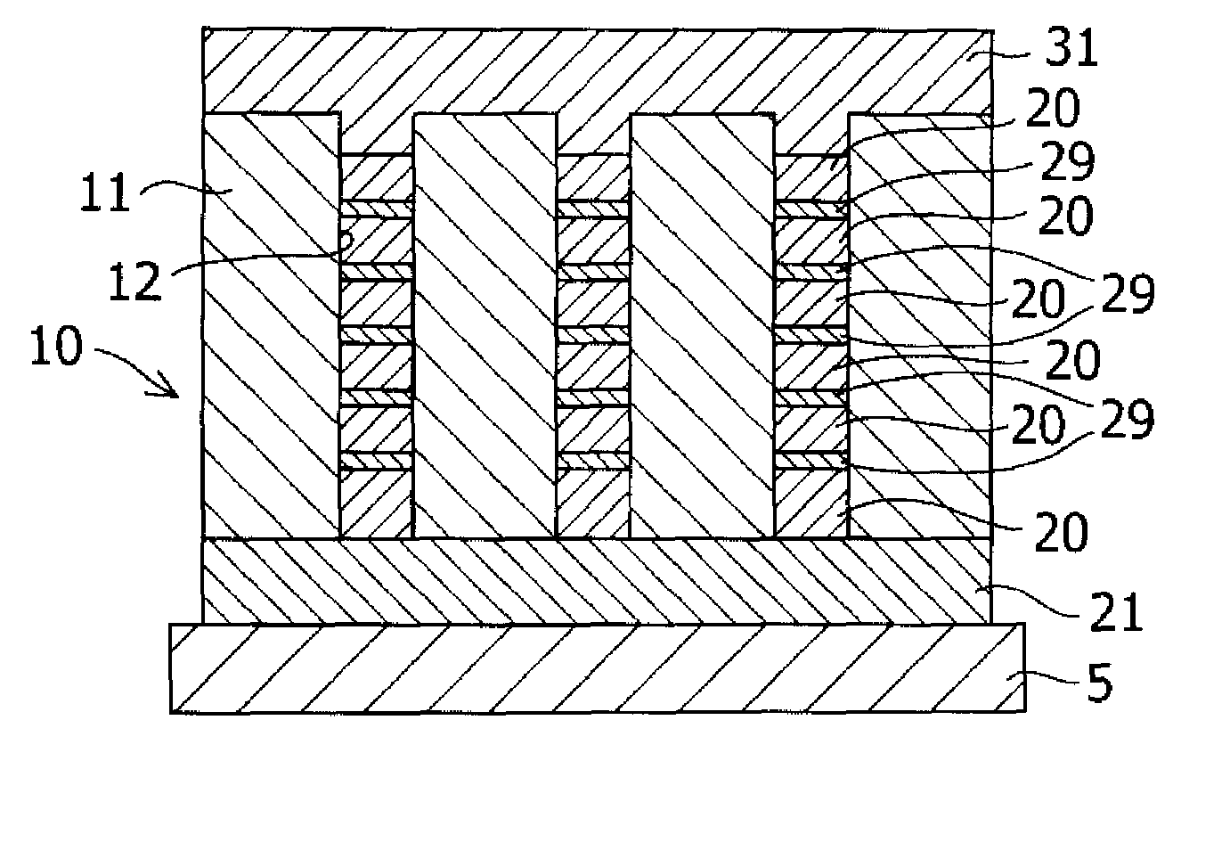
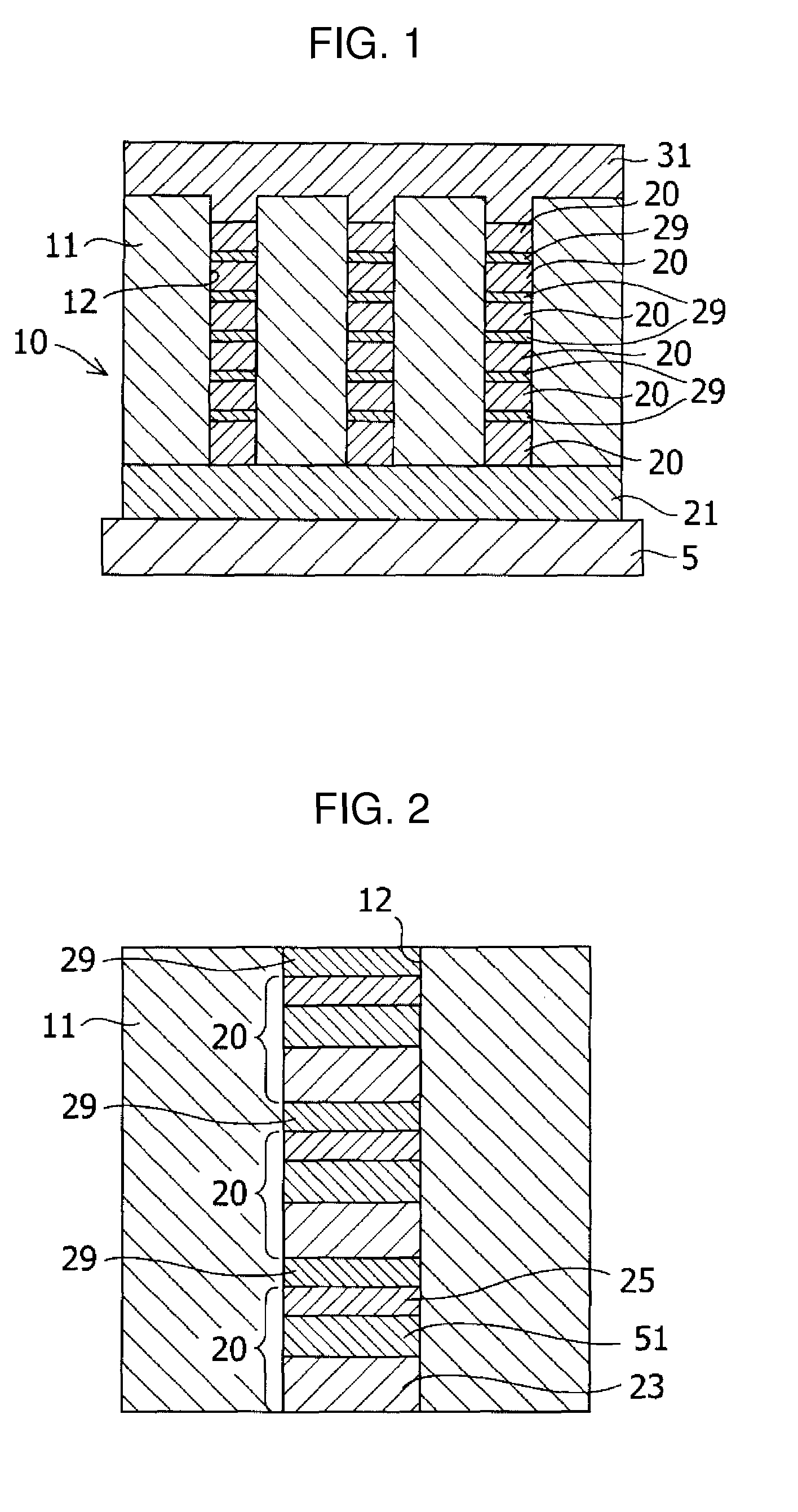
[0029]FIG. 1 is a vertical cross-sectional view showing the configuration of the spin valve element of a first embodiment of the invention, and FIG. 2 is an enlarged cross-sectional view of principal portions, showing the configuration of the spin valve element of the first embodiment. In this embodiment, as shown in the figures, a plurality of spin valve layers 20 are layered in a plurality of minute holes 12 formed in the insulating member 11 in a porous insulating layer 10 so as to be series-connected, and these can be connected in parallel by an electrode 31 and an electrode layer 21. Here, layered portions are shown in the figures, but in this invention a configuration is also possible in which a single spin valve layer 20 in the minute holes 12 is placed in each minute hole 12, and layering is not performed. The following description takes as an example a case in which the spin valve layers 20 have a GMR structure, but similar functions can be obtained in this embodiment even ...
second embodiment
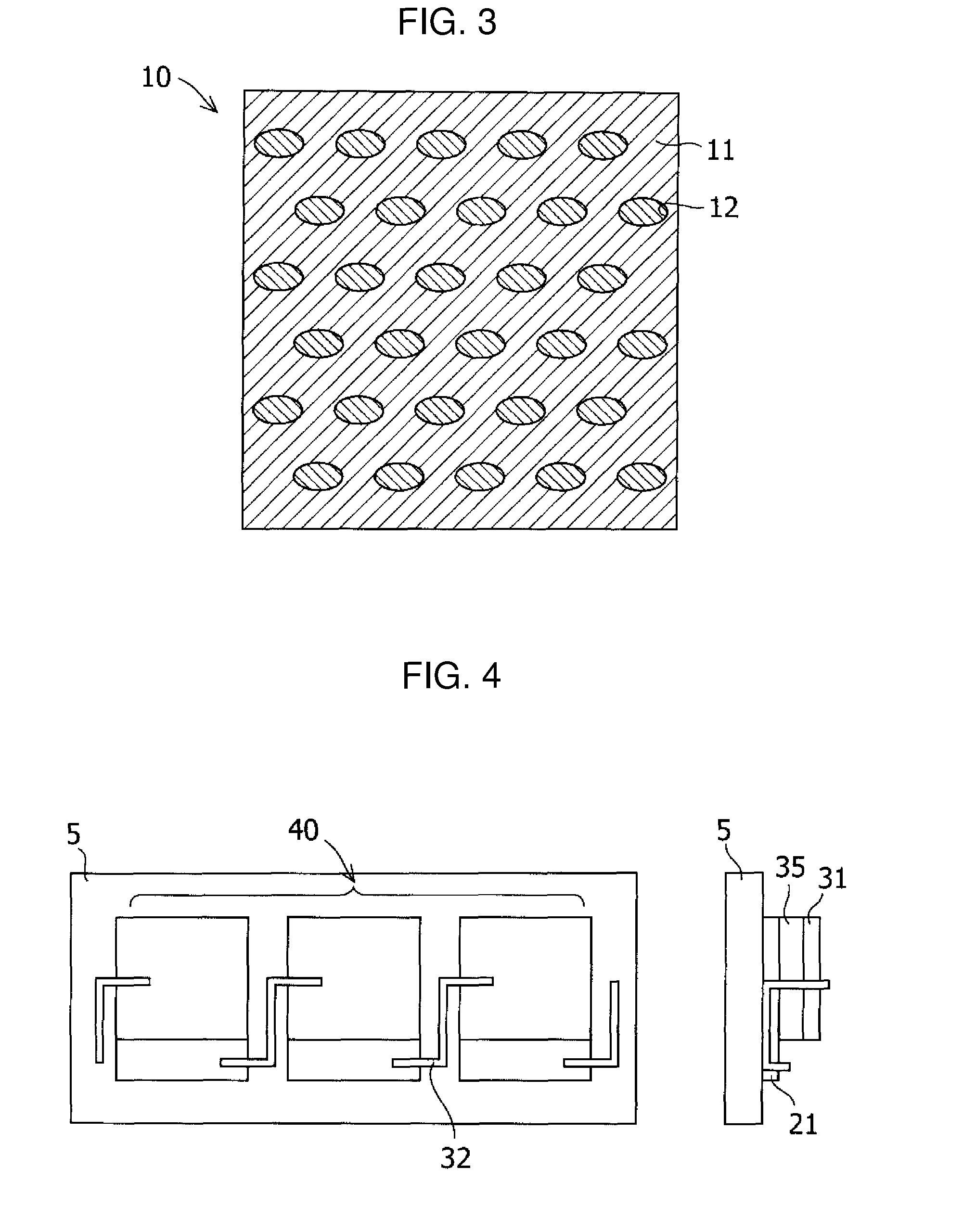
[0048]FIG. 4 shows one example of the spin valve element of a second embodiment of the invention. In the spin valve element of the second embodiment, integrated spin valve elements, obtained for example by the above method, are separated into island shapes approximately several micrometers on a side on a substrate, within a range which overall is approximately 100 μm. And, these spin valve elements are connected in parallel or in series on the substrate, and the entirety is used as a spin valve element. As explained above, the dimensions of separate spin valve elements (magnetic elements) must be approximately 150 nm or less, and the wiring between these elements requires expensive investments in electron beam exposure or other equipment. The second embodiment of the invention adopts a configuration in which a spin valve element group, in which are integrated several hundred to several thousand elements, are formed at once, and a plurality of element groups are provided and these gr...
example 1
Practical Example 1
[0053]Using the structure of the First Embodiment, a TMR layer was first fabricated by the following procedure. Following each of the materials, the film thickness of the layer is indicated in parentheses. A Cu (80 nm) thin film was formed on the silicon substrate 5 by a sputtering method as the electrode layer 21. Then, CO20Fe30 (20 nm) as the ferromagnetic layer 23, MgO (0.6 nm) as the insulating layer 24, CO40Fe40B20 (2 nm) as the ferromagnetic layer 25, Cu (2 nm) as the capping layer (not shown), and Pt (10 nm) as the intermediate electrode layer 29, were layered in order, to obtain one spin valve layer 20. And, by repeating this process, a total of five spin valve layers were layered.
[0054]Next, negative resist was applied onto the uppermost face of the spin valve layers, and elliptical regions were irradiated with an electron beam so as to form regions arranged in a honeycomb pattern of ellipses with major axis of 120 nm×minor axis of 60 nm, and with hole ce...
PUM
| Property | Measurement | Unit |
|---|---|---|
| Electrical conductivity | aaaaa | aaaaa |
Abstract
Description
Claims
Application Information
 - R&D
- Intellectual Property
- Life Sciences
- Materials
- Tech Scout
- Unparalleled Data Quality
- Higher Quality Content
- 60% Fewer Hallucinations
Browse by: Latest US Patents, China's latest patents, Technical Efficacy Thesaurus, Application Domain, Technology Topic, Popular Technical Reports.
© 2025 PatSnap. All rights reserved.Legal|Privacy policy|Modern Slavery Act Transparency Statement|Sitemap|About US| Contact US: help@patsnap.com