Solid-state imaging device and method of manufacturing the same and electronic apparatus

a solid-state imaging and imaging device technology, applied in semiconductor devices, diodes, radiation controlled devices, etc., can solve the problems of snr deterioration with a decrease in pixel size, generation of electron traps, solid-state imaging devices, etc., to achieve the effect of improving the pixel property of the solid-state imaging device and improving the image quality

Active Publication Date: 2010-11-25
SONY SEMICON SOLUTIONS CORP
View PDF9 Cites 3 Cited by
  • Summary
  • Abstract
  • Description
  • Claims
  • Application Information

AI Technical Summary

Benefits of technology

[0017]In the solid-state imaging device according to an embodiment of the present invention, the silicide blocking layer is formed in the pixel section except for part or whole of an area above the isolation portion in the pixel section. Thus, the surface area of the silicide blocking layer decreases, reducing the degree of warping caused by a difference between the thermal expansion of the silicide blocking layer and the thermal expansion of the semiconductor substrate. It leads to reduced warping stress, suppressing the generation of any stress-induced noise. Since no metal silicide layer is formed in the pixel section, the generation of junction leakage, dark current, and white spot can be suppressed.
[0019]According to the method of manufacturing a solid-state imaging device of the embodiment of the present invention, the area covered by the silicide blocking layer can be reduced by including the step of selectively removing the silicide blocking layer from part or whole of an area above the isolation portion in the pixel section. Thus, the warping of the semiconductor substrate caused by a difference between the thermal expansion of the semiconductor substrate and the thermal expansion of the silicide blocking layer can be reduced in the subsequent thermal processing for silicidation. Furthermore, since the silicide blocking layer is formed in the area of the pixel section where it is required, the method allows the production of a solid-state imaging device in which the generation of junction leakage, dark current, and white spot are suppressed.
[0021]Since the electronic apparatus according to the above embodiment of the invention includes the solid-state imaging device according to the above embodiment of the present invention, image quality can be improved.
[0022]Therefore, according to any of the above embodiments of the present invention, the pixel property of the solid-state imaging device can be improved without increasing the number of manufacturing steps.

Problems solved by technology

Solid-state imaging devices may have a disadvantage in that SNR deteriorates with a decrease in pixel size.
Electrons flow out as the stress occurs, leading to the generation of electron traps and becoming a causal factor of noise generation.
However, if a metal silicide layer is formed on silicon in the pixel section, pixel property may be deteriorated because of an increase in junction leakage, dark current generation due to an influence received from the metal silicide layer, white spot generation, and so on.
Thus, solid-state imaging devices may have unsuitable pixel property due to the remaining silicide blocking layer on the pixel in the pixel section, or due to junction leakage, white spot, and so on caused by the silicidation of the pixel section.

Method used


Image

  • Solid-state imaging device and method of manufacturing the same and electronic apparatus
  • Solid-state imaging device and method of manufacturing the same and electronic apparatus
  • Solid-state imaging device and method of manufacturing the same and electronic apparatus

Examples


Embodiment Construction

[0037]Hereafter, embodiments of the present invention will be described in detail with reference to the attached drawings.

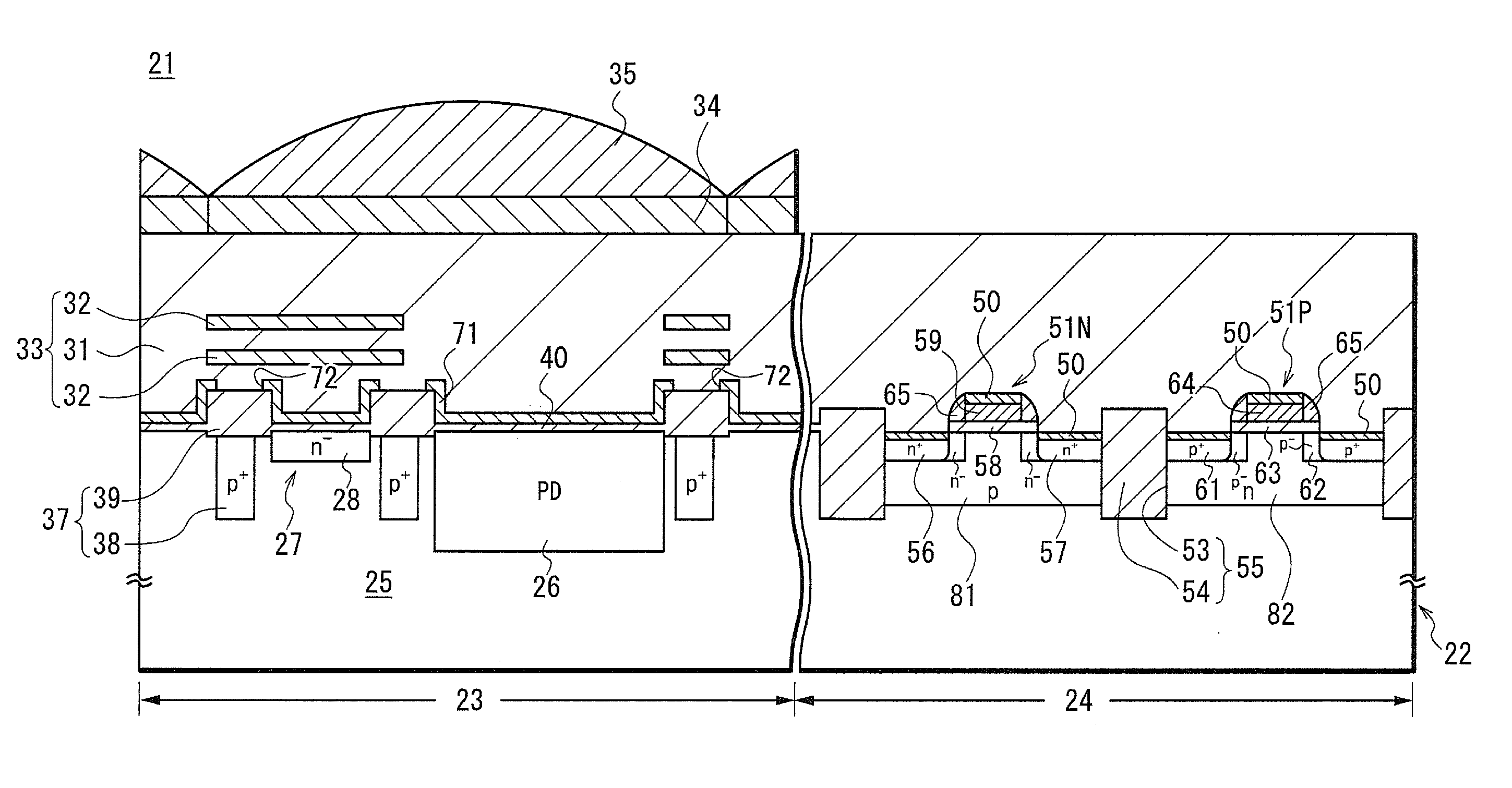
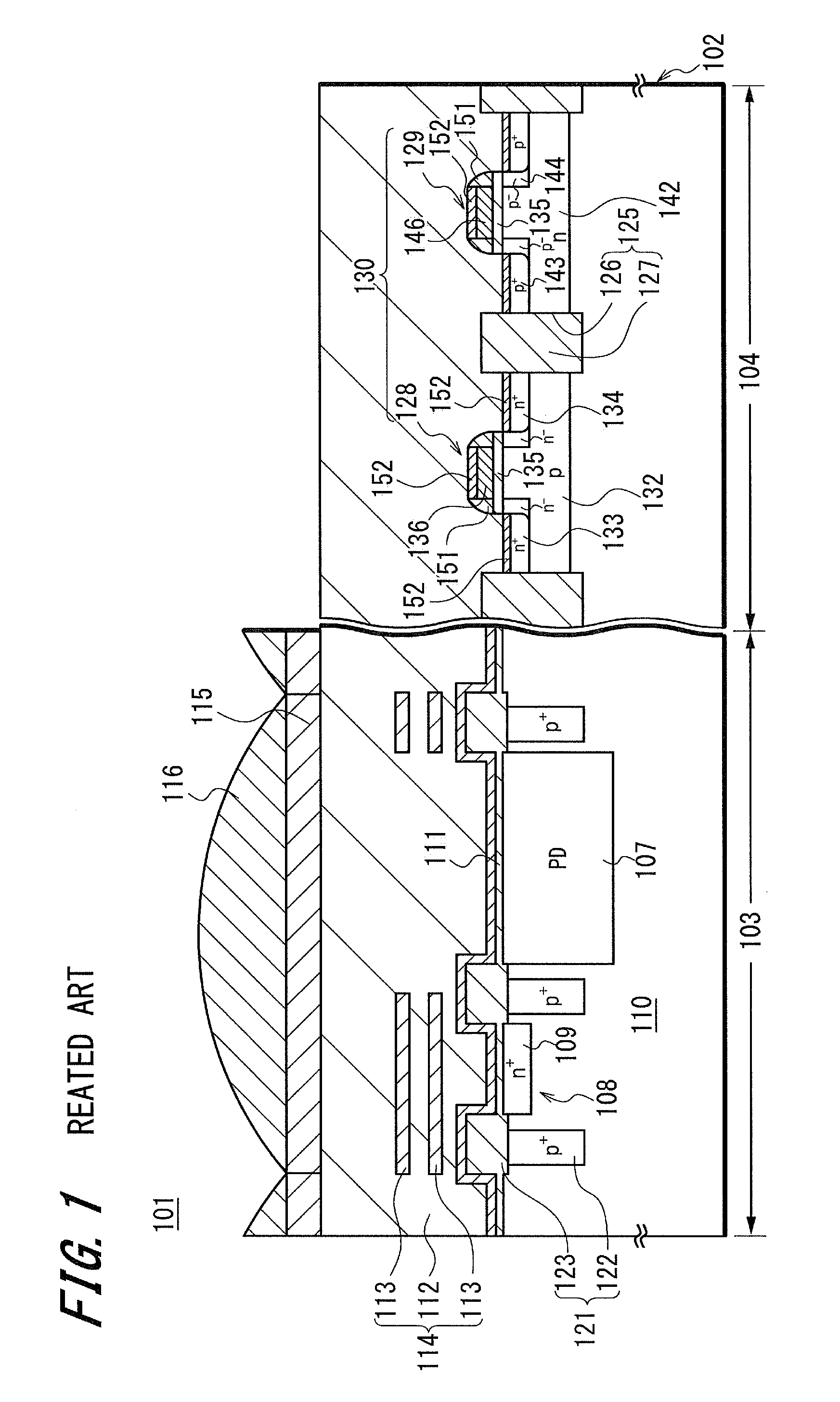
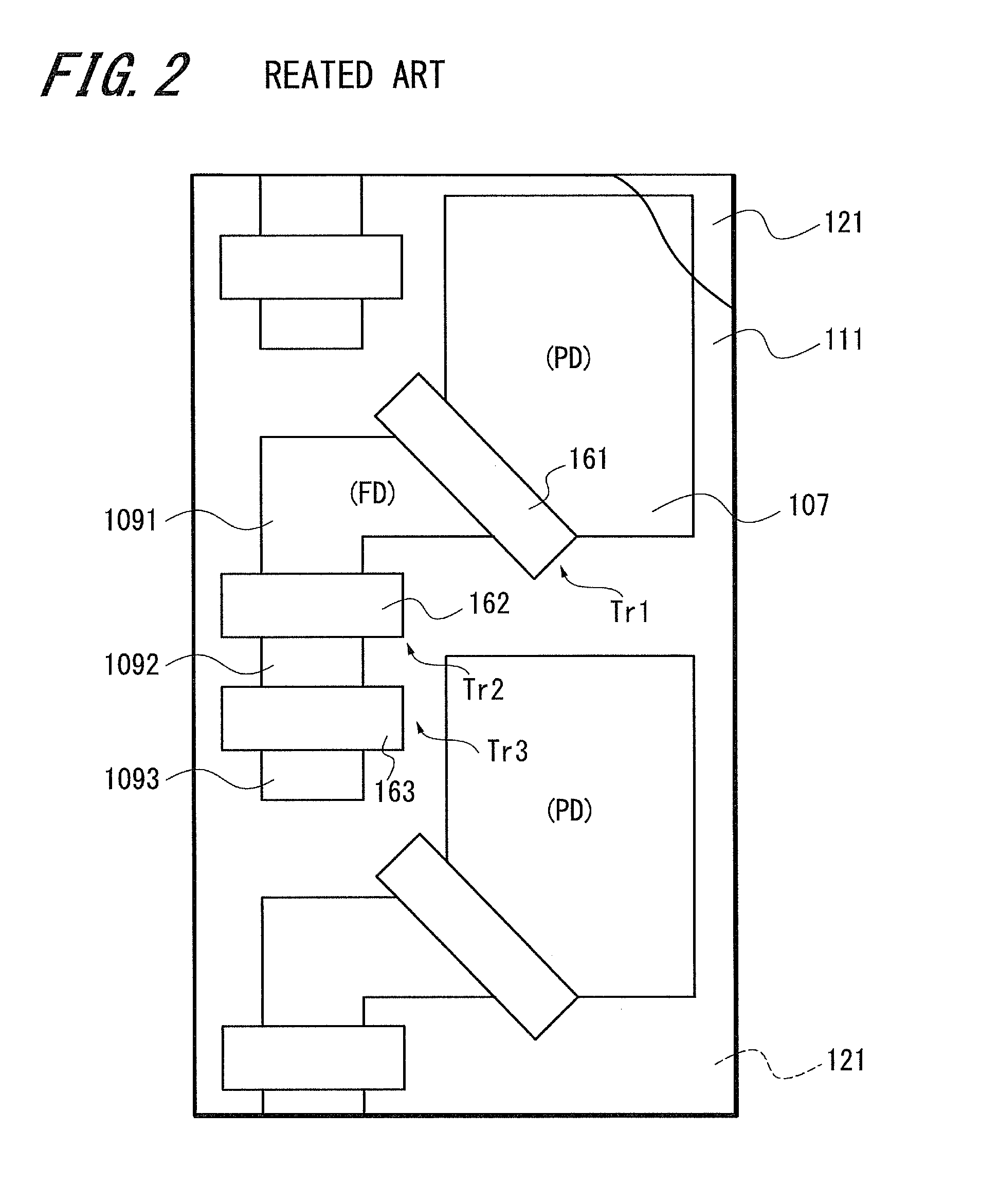
[0038]FIG. 3 is a schematic diagram illustrating an example configuration of a solid-state imaging device, or a CMOS solid-state imaging device, which can be applied to any embodiment of the present invention. A solid-state imaging device 1 includes a pixel section (imaging area) 3, where a plurality of pixels 2 with photoelectric conversion elements are regularly arranged in two dimension on a semiconductor substrate (e.g., a silicon substrate) 11; and a peripheral circuit section. Each pixel (i.e., unit pixel) 2 includes a photoelectric conversion element such as a photodiode and a plurality of pixel transistors (MOS transistors). The plurality of pixel transistors may be three transistors, for example, a transfer transistor, a reset transistor, and an amplification transistor. Alternatively, four transistors may be provided including an additional selection tr...


PUM


Abstract

A solid-state imaging device is provided. The solid-state imaging device includes a pixel section, a peripheral circuit section, a silicide blocking layer formed in the pixel section except for part or whole of an area above an isolation portion in the pixel section, and a metal-silicided transistor formed in the peripheral circuit section.

Description

RELATED APPLICATION DATA[0001]This application is a division of U.S. patent application Ser. No. 12 / 425,898, filed Apr. 17, 2009, the entirety of which is incorporated herein by reference to the extent permitted by law. The present application claims the benefit of priority to Japanese Patent Application No. 2008-110669 filed in the Japanese Patent Office on Apr. 21, 2008, the entirety of which is incorporated by reference herein to the extent permitted by law.BACKGROUND OF THE INVENTION[0002]1. Field of the Invention[0003]The present invention relates to a solid-state imaging device and a method of manufacturing such a solid-state imaging device, and also relates to an electronic apparatus including the solid-state imaging device.[0004]2. Description of the Related Art[0005]Solid-state imaging devices can be generally classified into those of an amplification-type typified by CMOS (Complementary Metal Oxide Semiconductor) image sensor and those of a charge-transfer type typified by...

Claims


Application Information

Patent Timeline
Patent Type & Authority Applications(United States)
IPC IPC(8): H01L27/146
CPCH01L27/14603H01L27/14609H01L27/1462H01L27/14621H01L27/14687H01L27/14627H01L27/1463H01L27/14643H01L27/14623
Inventor TATANI, KEIJI
Owner SONY SEMICON SOLUTIONS CORP
Why Eureka
Try Eureka