Mems-based pellicle beamsplitter
a beam splitter and pellicle technology, applied in the field of mems-based pellicle beam splitters, can solve the problems of inability to widely adopt circuit board manufacturing processes, inability to physically place fiber optics and connect fibers to chips, and inability to meet the requirements of inter-chip communication, etc., to achieve the effect of reducing circuit board routing, and increasing the complexity of optical signal routing
- Summary
- Abstract
- Description
- Claims
- Application Information
AI Technical Summary
Problems solved by technology
Method used
Image


Examples
embodiment 20
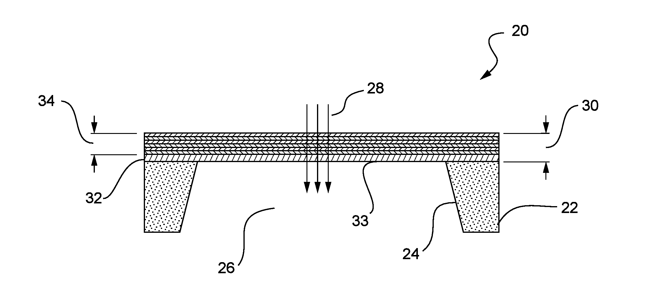
[0039]An application 40 of the pellicle beamsplitter into an optical waveguide with a single optical interconnect is shown in FIG. 5. A source 50 for an optical beam, such as a laser or LED, is situated at one end of the optical waveguide 60. The light source produces an incident light beam 52 which travels down the interior of the waveguide until contacting the pellicle beamsplitter 20, at which point a predetermined portion of the light is reflected into the optical interconnect 70 as the reflected optical beam 54, and a portion of the light is transmitted through the beamsplitter as the transmitted optical beam 56. The ratio of the reflected light energy over the incident light energy is known as the reflectance of the beamsplitter, and the ratio of the transmitted light energy over the incident light energy is known as the transmittance of the beamsplitter. The transmittance is also known as the power tap ratio.
[0040]One advantage of the present invention is that, through the pr...
embodiment 100
[0049]In another exemplary embodiment 100 of the present invention, one or more through-holes 124 or apertures can be formed in the pellicle membrane 110, as shown in FIGS. 10a-b. FIG. 10b, which is a partial view of the beamsplitter of FIG. 10a as viewed from section line B-B, shows that the through-holes can provide a continuous opening from the front surface 120 of the beamsplitter coating 114 to the back surface 122 of the base layer 112, which allows a portion of the incident light 128 striking the front (or back) surface of the membrane 110 to pass directly through the through-holes without contacting a physical surface. Furthermore, the plurality of layers having high and low indexes of refraction forming the beamsplitter coating 114 can be formed with sufficient reflectivity that substantially all light contacting the beamsplitter coating is reflected. As such, the pellicle membrane 110 of embodiment 100 reflects substantially all light that does not pass through the one or ...
embodiment 150
[0052]In another embodiment 150, as illustrated in FIGS. 12a-b, a slot 172 can be formed in the beamsplitter coating 164 to reduce any residual stresses in the coating which may cause it to bow or ripple or otherwise deform in a manner that may affect the optical pathway. The slot may extend from the top surface of the pellicle membrane 160 all the way through the beamsplitter coating until reaching the base layer 162, but would not extend through the base layer. Furthermore, the slot may completely encircle a center region of the pellicle membrane, as shown, or may extend only partway around an exterior portion of the membrane, or may be broken up into multiple separate and discrete slots located as needed around the center region of the membrane. Moreover, the slot can assume any shape, such as a square, rectangle or circle, and can also be formed using any lithographic or similar manufacturing technique.
PUM
 Abstract
Description
Claims
Application Information
 - R&D
- Intellectual Property
- Life Sciences
- Materials
- Tech Scout
- Unparalleled Data Quality
- Higher Quality Content
- 60% Fewer Hallucinations
Browse by: Latest US Patents, China's latest patents, Technical Efficacy Thesaurus, Application Domain, Technology Topic, Popular Technical Reports.
© 2025 PatSnap. All rights reserved.Legal|Privacy policy|Modern Slavery Act Transparency Statement|Sitemap|About US| Contact US: help@patsnap.com