Three-dimensional thin-film semiconductor substrate with through-holes and methods of manufacturing

a technology of semiconductor substrates and throughholes, applied in the field of photovoltaics and solar cells, can solve the problems of low efficiency of bipv modules standard crystalline semiconductors, and achieve the effect of reducing disadvantages and problems

Inactive Publication Date: 2010-12-02
BEAMREACH SOLAR INC
View PDF99 Cites 65 Cited by
  • Summary
  • Abstract
  • Description
  • Claims
  • Application Information

AI Technical Summary

Benefits of technology

[0011]In accordance with the present disclosure, methods for manufacturing three-dimensional thin-film solar cells (3-D TFSCs) are provided. The 3-D TFSCs of the disclosed subject matter substantially eliminate or reduce disadvantages and problems associated with previously developed semiconductor wafer-based solar cells as well as TFSCs, both in terms of conversion efficiency as well as manufacturing costs.

Problems solved by technology

However, these TF technologies in practice offer efficiencies in the range of 5% to 12%, with the TF see-through BIPV module efficiencies being essentially limited to the single-digit efficiency range of 4% to 8%.
While this see-through crystalline semiconductor PV modules can provide relatively high effective efficiencies (e.g., typically in the range of 10% to 12%), they do not offer very attractive aesthetics, both due to the tiled design and also due to the standard busbar emitter interconnects in the cells (thus, showing visible metallization fingers and busbars).
This is far below the efficiency of standard crystalline semiconductor BIPV modules.
OPV and DSSC BIPV modules cannot easily compete with the conventional crystalline semiconductor or TF BIPV solar panels due to their relatively low conversion efficiencies and shorter operational lifetimes. Crystalline semiconductor solar cells and modules have proven long lifetimes in excess of 25-30 years in the field and no TF or DSSC technology can offer or match such track record.

Method used


Image

  • Three-dimensional thin-film semiconductor substrate with through-holes and methods of manufacturing
  • Three-dimensional thin-film semiconductor substrate with through-holes and methods of manufacturing
  • Three-dimensional thin-film semiconductor substrate with through-holes and methods of manufacturing

Examples


Embodiment Construction

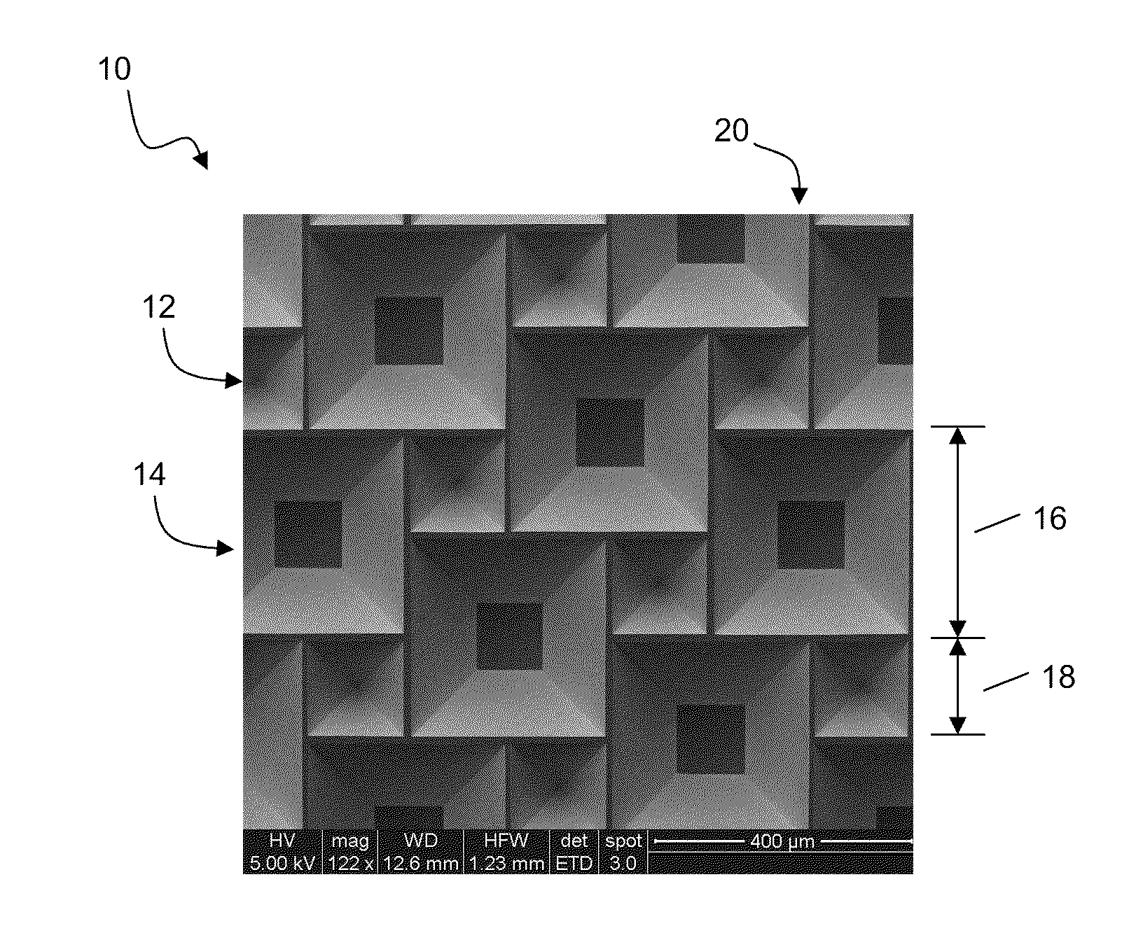
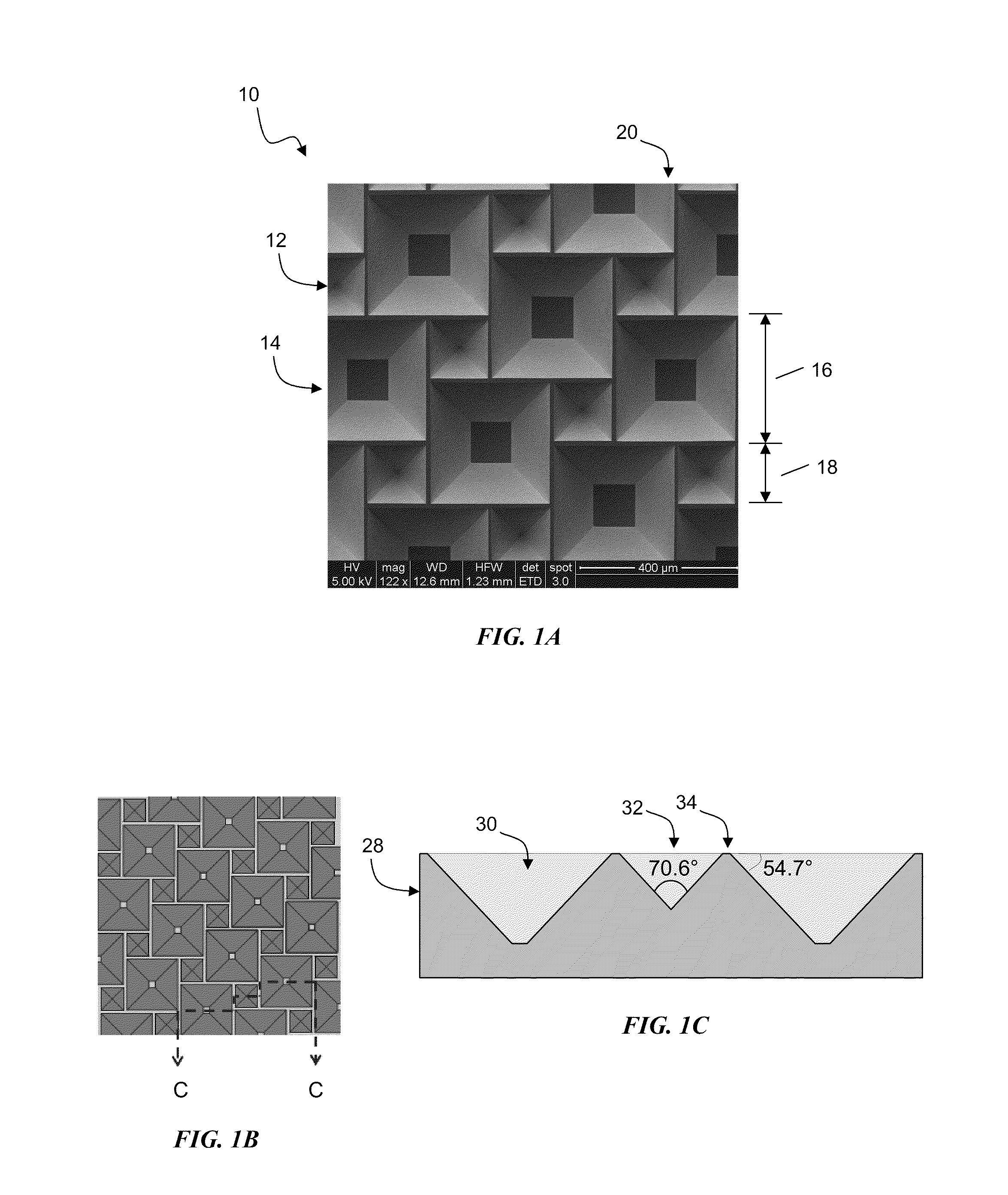
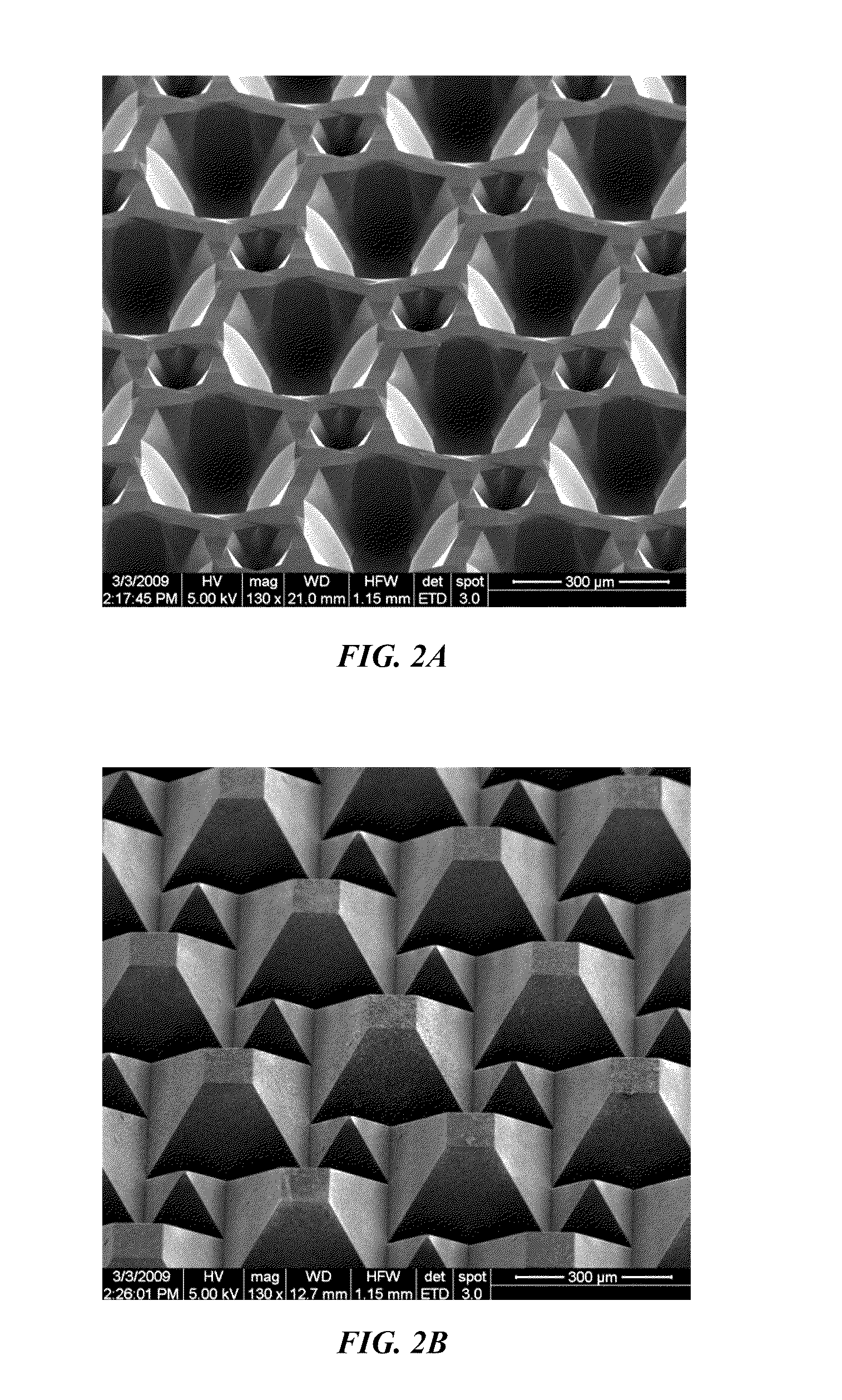
[0052]The following description is not to be taken in a limiting sense, but is made for the purpose of describing the general principles of the present disclosure. The scope of the present disclosure should be determined with reference to the claims. Exemplary embodiments of the present disclosure are illustrated in the drawings, like numbers being used to refer to like and corresponding parts of the various drawings.

[0053]Although described with reference to specific embodiments, one skilled in the art could apply the principles discussed herein to other areas and / or embodiments. A preferred semiconductor material for the 3-D TFSS is crystalline silicon (c-Si), although other semiconductor materials may also be used. One embodiment uses monocrystalline silicon as the thin film semiconductor material. Other embodiments use multicrystalline silicon, polycrystalline silicon, microcrystalline silicon, amorphous silicon, porous silicon, and / or a combination thereof. The designs here are...


PUM


Abstract

A method for the fabrication of a three-dimensional thin-film semiconductor substrate with selective through-holes is provided. A porous semiconductor layer is conformally formed on a semiconductor template comprising a plurality of three-dimensional inverted pyramidal surface features defined by top surface areas aligned along a (100) crystallographic orientation plane of the semiconductor template and a plurality of inverted pyramidal cavities defined by sidewalls aligned along the (111) crystallographic orientation plane of the semiconductor template. An epitaxial semiconductor layer is conformally formed on the porous semiconductor layer. The epitaxial semiconductor layer is released from the semiconductor template. Through-holes are selectively formed in the epitaxial semiconductor layer with openings between the front and back lateral surface planes of the epitaxial semiconductor layer to form a partially transparent three-dimensional thin-film semiconductor substrate.

Description

CROSS-REFERENCE TO RELATED APPLICATIONS[0001]This application claims the benefit of provisional patent application 61 / 182,635 filed on May 29, 2009, which is hereby incorporated by reference in its entirety.[0002]This application also claims the benefit of provisional patent application 61 / 228,068 filed on Jul. 23, 2009, which is hereby incorporated by reference in its entirety.FIELD OF THE INVENTION[0003]This disclosure relates in general to the field of photovoltaics and solar cells, and more particularly to semiconductor substrates and methods for making semiconductor substrates with through-holes for use in manufacturing three-dimensional thin-film solar cells.BACKGROUND OF THE INVENTION[0004]Building-Integrated Photovoltaics (BIPV) involves the process of integrating energy (electricity) producing photovoltaic technology into residential, commercial, and industrial building and construction design and materials. By using BIPV, the solar electricity producing components actually...

Claims


Application Information

Patent Timeline
Patent Type & Authority Applications(United States)
IPC IPC(8): H01L31/0352H01L31/18
CPCH01L31/035281H01L31/1804Y02E10/547H01L31/03529H01L31/1892H01L31/054H01L31/056H01L27/142H01L31/0468Y02E10/52Y02P70/50H01L21/00H01L31/0352
Inventor MOSLEHI, MEHRDAD M.WANG, DAVID XUAN-QI
Owner BEAMREACH SOLAR INC
Why Eureka
Try Eureka