Semiconductor device and method for manufacturing the same

a semiconductor and semiconductor technology, applied in the direction of semiconductor devices, electrical equipment, transistors, etc., can solve the problems of difficult circuit control, poor interface characteristics, and inability to perform switching functions, etc., to prevent hillocks, improve heat resistance, and excellent interface characteristics

Active Publication Date: 2010-12-02
SEMICON ENERGY LAB CO LTD
View PDF106 Cites 97 Cited by
  • Summary
  • Abstract
  • Description
  • Claims
  • Application Information

AI Technical Summary

Benefits of technology

[0020]The field effect mobility of a thin film transistor in which a channel formation region is provided in an oxide semiconductor is higher than that of a thin film transistor using amorphous silicon.

Problems solved by technology

When the threshold voltage value is high or is on the minus side, it is difficult to control the circuit even if the field effect mobility is high.
When a thin film transistor has high threshold voltage value and a large absolute value of its threshold voltage, the TFT cannot perform switching function and may be a load when driven at low voltage.
A transistor in which a channel is not formed unless a high driving voltage is applied and a transistor in which a channel is formed and drain current flows even in the case of the negative voltage state are unsuitable for a thin film transistor used in a circuit.

Method used


Image

  • Semiconductor device and method for manufacturing the same
  • Semiconductor device and method for manufacturing the same
  • Semiconductor device and method for manufacturing the same

Examples


embodiment 1

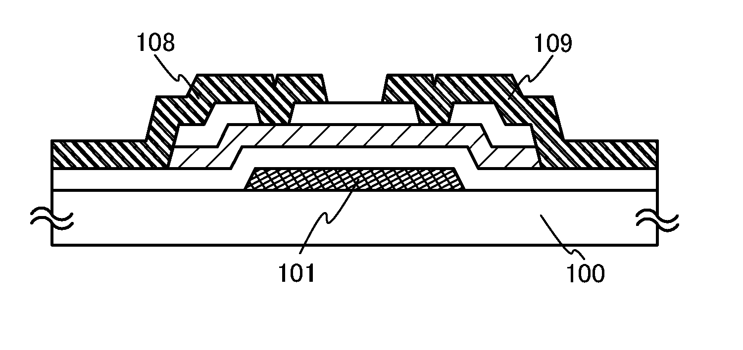
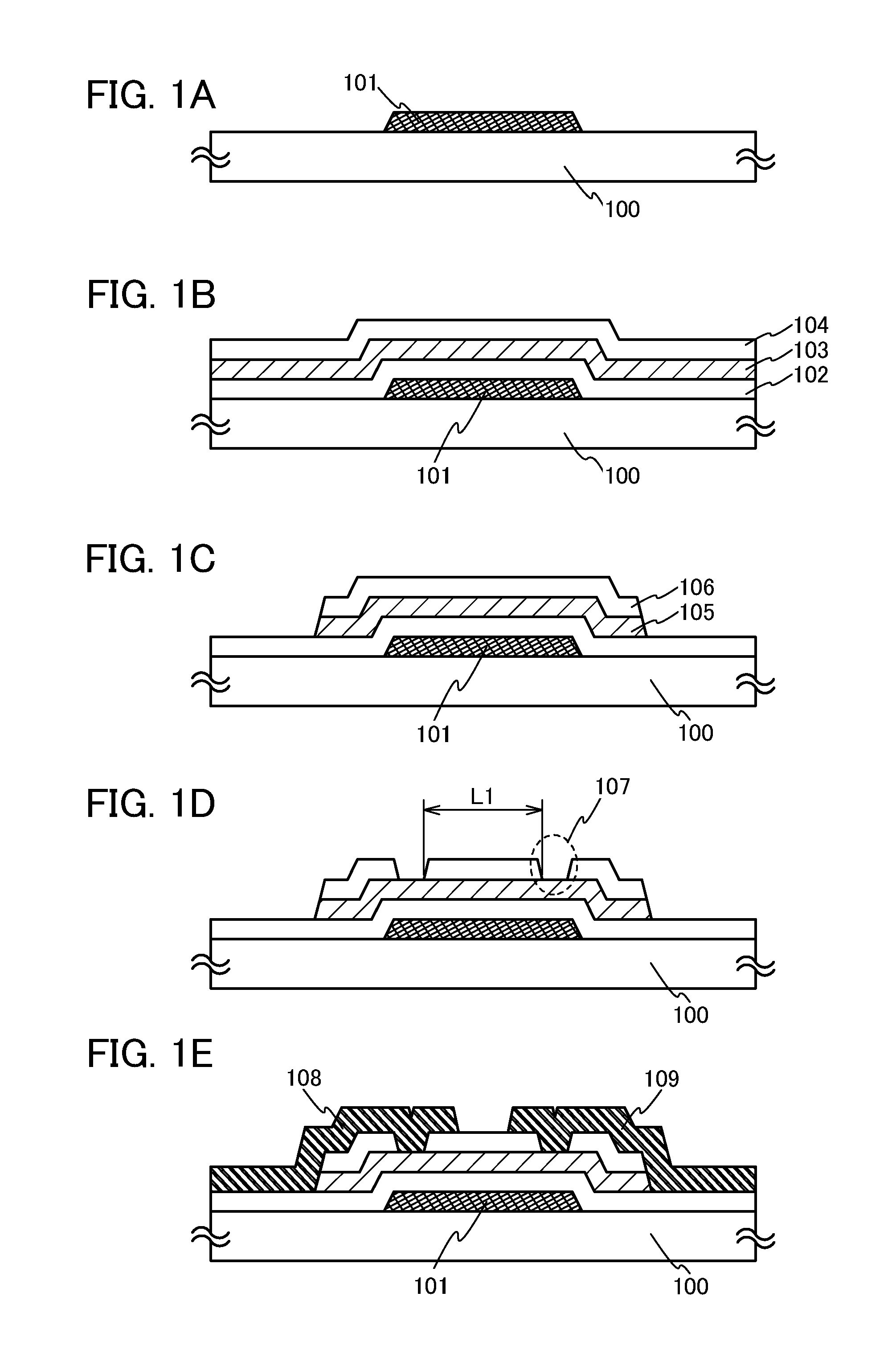
[0089]In this embodiment, a thin film transistor and a manufacturing process thereof will be described with reference to FIGS. 1A to 1E.

[0090]First, a gate electrode 101 is formed over a substrate 100 (see FIG. 1A).

[0091]As the substrate 100, any of the following substrates can be used: non-alkaline glass substrates formed of barium borosilicate glass, aluminoborosilicate glass, aluminosilicate glass, and the like with a fusion method or a float method; ceramic substrates; plastic substrates having heat resistance sufficient to withstand a process temperature of this manufacturing process; and the like. Alternatively, a metal substrate such as a stainless steel alloy substrate which is provided with an insulating film over the surface may be used. As the substrate 100, a substrate having a size of 320 mm×400 mm, 370 mm×470 mm, 550 mm×650 mm, 600 mm×720 mm, 680 mm×880 mm, 730 mm×920 mm, 1000 mm×1200 mm, 1100 mm×1250 mm, 1150 mm×1300 mm, 1500 mm×1800 mm, 1900 mm×2200 mm, 2160 mm×2460 ...

embodiment 2

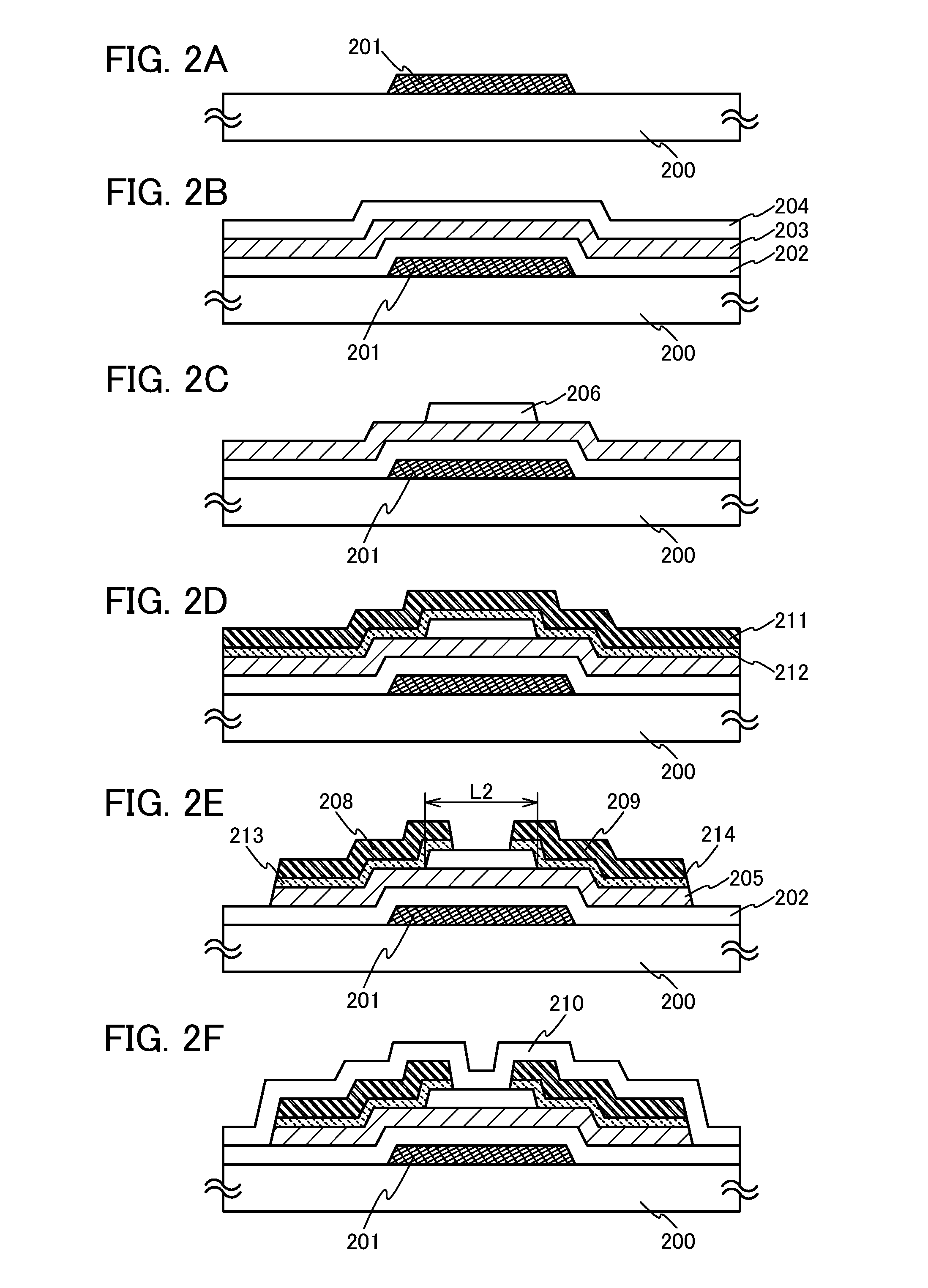
[0114]In this embodiment, a thin film transistor and a manufacturing process thereof will be described with reference to FIGS. 2A to 2F. Note that repetitive description of the same portions as Embodiment 1 or portions having functions similar to those in Embodiment 1, and steps for forming such portions will be omitted.

[0115]First, a gate electrode 201 is formed over a substrate 200. Here, a first photomask is used (see FIG. 2A).

[0116]Next, a first insulating film 202 serving as a gate insulating film, a first semiconductor film 203, and a second insulating film 204 are successively formed without being exposed to air (see FIG. 2B). Here, as the first insulating film 202 and the second insulating film 204, silicon oxynitride films each including nitrogen at greater than or equal to 3 atomic % and less than or equal to 30 atomic % are formed with an RF sputtering method. As the first semiconductor film 203, an oxide semiconductor layer is formed with a DC magnetron sputtering method...

embodiment 3

[0127]In this embodiment, a thin film transistor and a manufacturing process thereof will be described with reference to FIGS. 3A to 3E. Note that repetitive description of the same portions as Embodiment 1 or portions having functions similar to those in Embodiment 1, and steps for forming such portions will be omitted.

[0128]First, a gate electrode 301 is formed over a substrate 300. Here, a first photomask is used.

[0129]Next, a first insulating film 302, serving as a gate insulating film, and a metal multilayer film 311, serving as a source electrode and a drain electrode, are formed.

[0130]The first insulating film 302 can be formed using a silicon oxide film, a silicon nitride film, a silicon oxynitride film, or a silicon nitride oxide film with a CVD method, a sputtering method, or the like. Here, a silicon oxynitride film including nitrogen at greater than or equal to 3 atomic % and less than or equal to 30 atomic % is formed as the first insulating film 302 with an RF sputteri...


PUM


Abstract

Homogeneity and stability of electric characteristics of a thin film transistor included in a circuit are critical for the performance of a display device including said circuit. An object of the invention is to provide an oxide semiconductor film with low hydrogen content and which is used in an inverted staggered thin film transistor having well defined electric characteristics. In order to achieve the object, a gate insulating film, an oxide semiconductor layer, and a channel protective film are successively formed with a sputtering method without being exposed to air. The oxide semiconductor layer is formed so as to limit hydrogen contamination, in an atmosphere including a proportion of oxygen. In addition, layers provided over and under a channel formation region of the oxide semiconductor layer are formed using compounds of silicon, oxygen and / or nitrogen.

Description

BACKGROUND OF THE INVENTION[0001]1. Field of the Invention[0002]The present invention relates to a semiconductor device which has a circuit including a thin film transistor (hereinafter also referred to as a TFT) in which a channel formation region is formed using an oxide semiconductor film and a method for manufacturing the semiconductor device. For example, the present invention relates to an electronic device having an electro-optical device typified by a liquid crystal display panel or a light-emitting display device including an organic light-emitting element.[0003]It is to be noted that the semiconductor device in this specification refers to all devices that can function by utilizing semiconductor characteristics, and electro-optical devices, semiconductor circuits, and electronic devices are all semiconductor devices.[0004]2. Description of the Related Art[0005]Various metal oxides are used for a variety of applications. Indium oxide is a well-known material and is used as ...

Claims


Application Information

Patent Timeline
Patent Type & Authority Applications(United States)
IPC IPC(8): H01L29/786H01L29/02H01L21/04H01L21/34
CPCH01L27/1225H01L29/4908H01L29/78609H01L29/7869H01L29/78693H01L29/24H01L29/247H01L29/513H01L29/78696H01L29/66742H01L29/786H01L29/78606H01L27/1248
Inventor YAMAZAKI, SHUNPEIAKIMOTO, KENGO
Owner SEMICON ENERGY LAB CO LTD
Why Eureka
Try Eureka