Semiconductor integrated circuit device

a technology of integrated circuit devices and semiconductors, applied in the direction of semiconductor integrated circuit devices, emergency protective arrangements for limiting excess voltage/current, electrical equipment, etc., can solve the problems of increasing costs, achieve the effect of improving the performance of the semiconductor integrated circuit device, increasing the current absorption capacity, and substantially reducing the layout required for the esd protection circui

Inactive Publication Date: 2010-12-02
RENESAS ELECTRONICS CORP
View PDF6 Cites 22 Cited by
  • Summary
  • Abstract
  • Description
  • Claims
  • Application Information

AI Technical Summary

Benefits of technology

[0029](1) The current absorption capacity can be increased while layout required for the ESD protection circuit is substantially decreased.
[0030](2) The above advantage allows securing a high-pe

Problems solved by technology

As described above, in recent years, a demand for a high ESD withstand voltage and an increase in the number of high withstand voltage terminals i

Method used


Image

  • Semiconductor integrated circuit device
  • Semiconductor integrated circuit device
  • Semiconductor integrated circuit device

Examples


Embodiment Construction

[0040]The embodiment of the present invention is described in detail below with reference to the drawings. The similar components in all the drawings for describing the embodiment are designated by the same reference numerals and characters in principle to omit the description thereof.

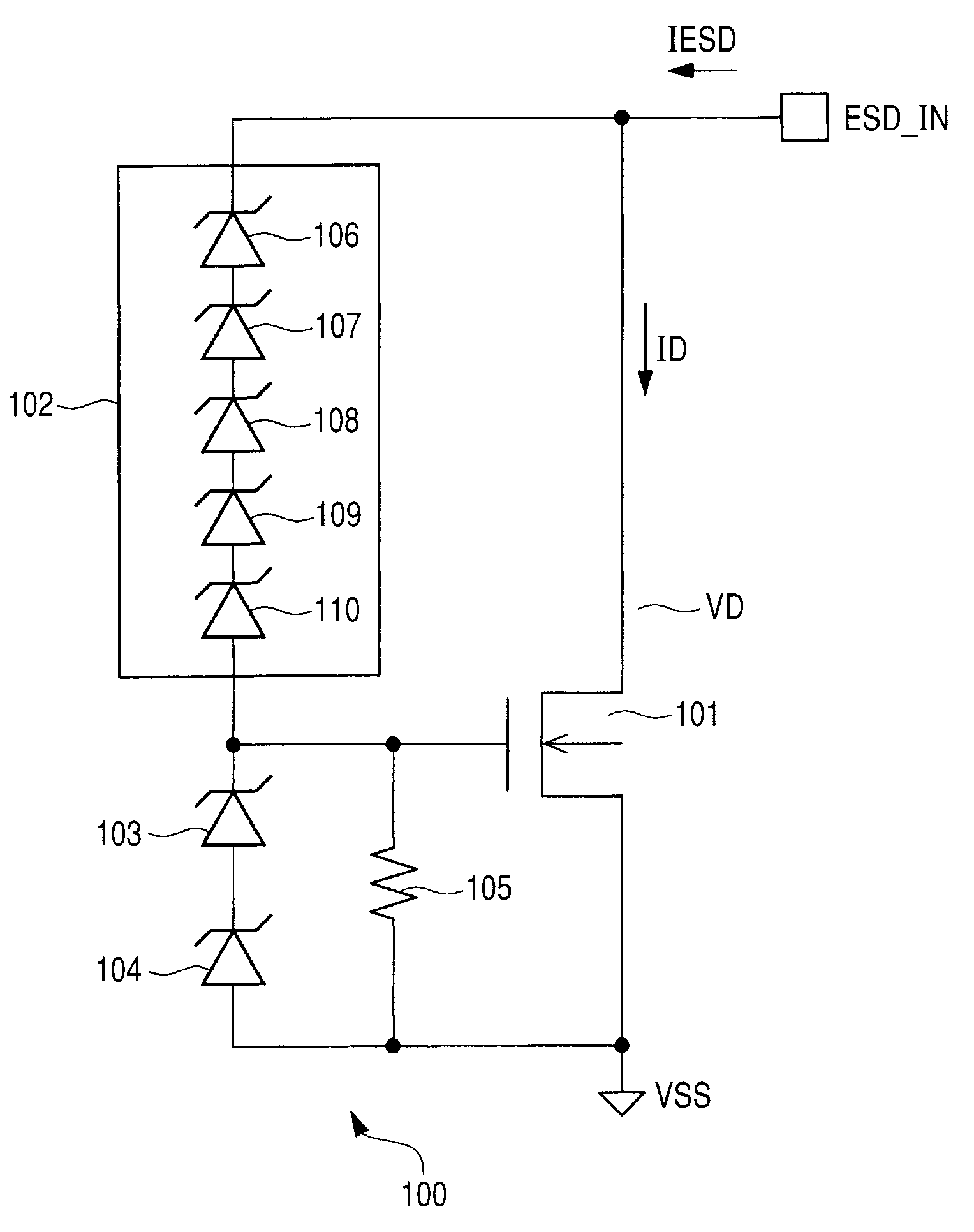
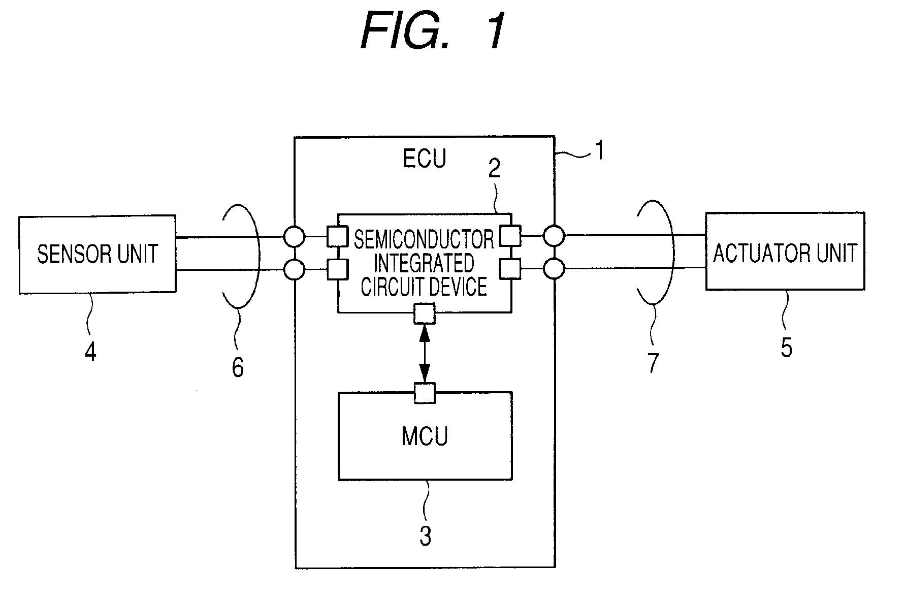
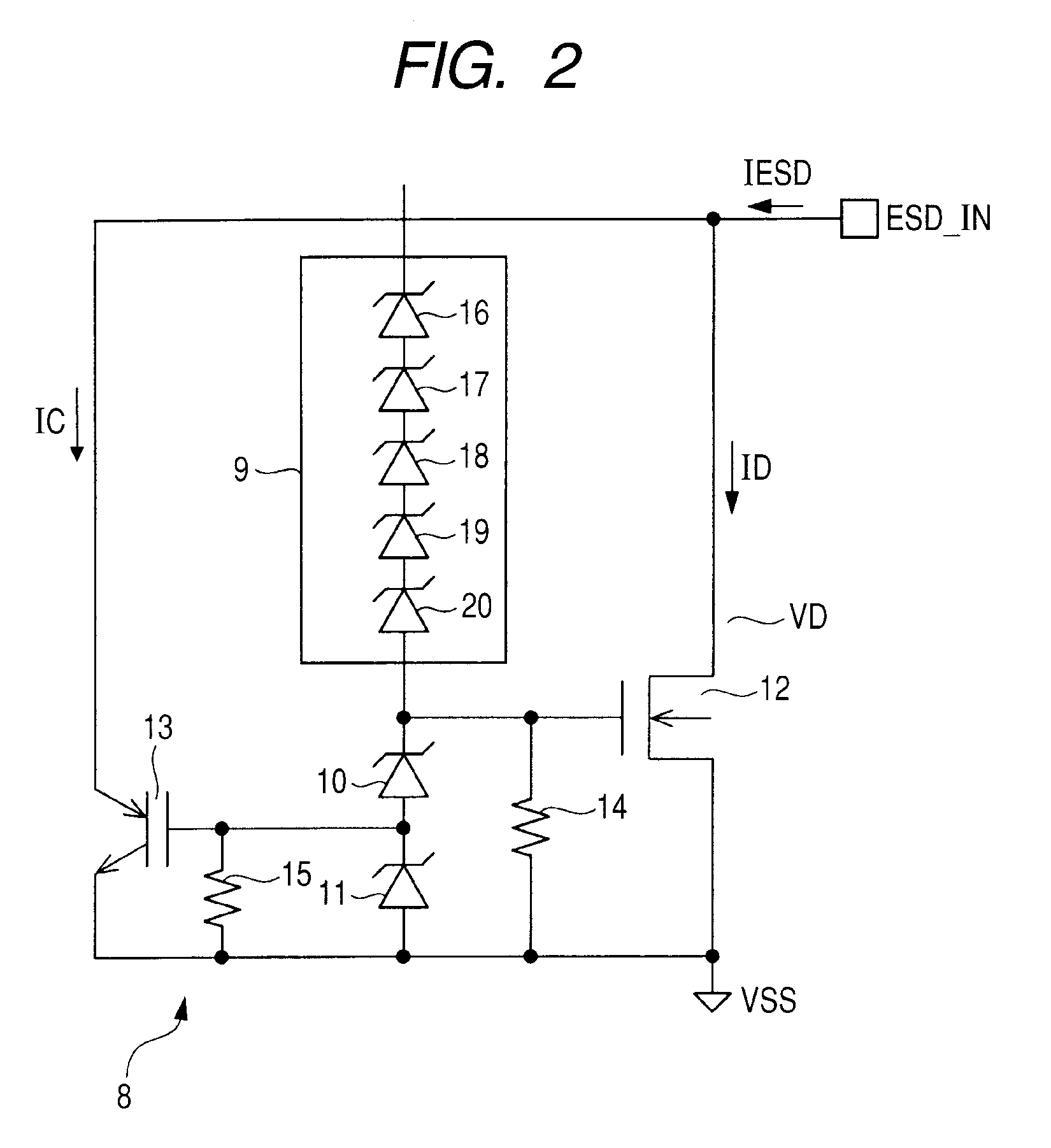
[0041]FIG. 1 is a block diagram showing an example of an ECU module according to a first embodiment of the present invention. FIG. 2 is a circuit diagram showing an example of an ESD protection circuit provided in the semiconductor integrated circuit device in FIG. 1. FIG. 3 is a chart showing an example of an electrical characteristic of a transistor comprised of a DMOS provided in the ESD protection circuit in FIG. 2. FIG. 4 is a chart showing an example of an electrical characteristic of a transistor comprised of an IGBT provided in the ESD protection circuit in FIG. 2. FIG. 5 is a chart showing an example of an electrical characteristic in the ESD protection circuit in FIG. 2. FIG. 6 is a cross sec...


PUM


Abstract

The present invention provides a technique capable of realizing an ESD protection performance having a high ESD withstand voltage in a small layout area. An ESD protection circuit includes a clamping circuit, Zener diodes, a transistor comprised of a DMOS, a transistor comprised of an IGBT, and resistors. The ESD protection circuit effectively protects the protected circuit such that the transistor comprised of the DMOS is caused to absorb the current noise at the time of operating the protected circuit to prevent malfunction due to latchup and the IGBT (the transistor comprised of IGBT) whose current absorption capacity is increased by the thyristor effect is operated in parallel for a large current at the time of ESD.

Description

CROSS-REFERENCE TO RELATED APPLICATIONS[0001]The disclosure of Japanese Patent Application No. 2009-128612 filed on May 28, 2009 including the specification, drawings and abstract is incorporated herein by reference in its entirety.BACKGROUND OF THE INVENTION[0002]The present invention relates to an electrostatic discharge (ESD) protection technique in a semiconductor integrated circuit device and, in particular, to an effective technique for ESD protection in a semiconductor integrated circuit device including a high voltage terminal to which a high voltage is applied.[0003]In recent years, there has been growing demand for ESD withstand voltage for a high voltage terminal in a semiconductor integrated circuit device. Particularly, in an automobile, there has been growing demand for ESD withstand voltage in a semiconductor integrated circuit device to improve reliability and reduce the number of ESD protection components on an ECU.[0004]For example, in an on-vehicle electronic cont...

Claims


Application Information

Patent Timeline
IPC IPC(8): H02H9/00
CPCH01L27/0251H01L29/0834H01L29/0878H01L29/7393H01L29/7816H02H9/046
Inventor HAYASHI, YUTAKA
Owner RENESAS ELECTRONICS CORP
Why Eureka
Try Eureka