Semiconductor device and method of manufacturing semiconductor device

Active Publication Date: 2010-12-09
NICHIA CORP
View PDF9 Cites 12 Cited by
  • Summary
  • Abstract
  • Description
  • Claims
  • Application Information

AI Technical Summary

Benefits of technology

[0028]A semiconductor device according to the present invention is capable of preventing light absorption by an electrode, so that a semiconductor device with improved reliability can be obtained.
[0029]Also, according to a manufacturing method of a semiconductor d

Problems solved by technology

For example, in a case where a material such as GaAs is used, due to its low contact resistivity, its effects on the laser operating characteristics is hardly expected even if the contact area between the upper surface of the stripe-shaped ridge and the electrode is changed, and a meaningful increase in laser operating voltage is unlikely to occur.
Whereas, in a case where a material made of a nitride semiconductor such as GaN is used, due to its higher contact resistivity compared to that of GaAs, the contact resistivity between the electrode and the upper surface of the ridge may be increased according to a change in the contact area between the upper surface of the ridge and the electrode, which may results

Method used


Image

  • Semiconductor device and method of manufacturing semiconductor device
  • Semiconductor device and method of manufacturing semiconductor device
  • Semiconductor device and method of manufacturing semiconductor device

Examples


example 1

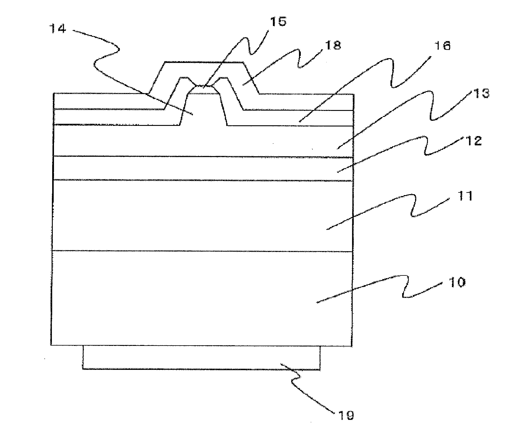
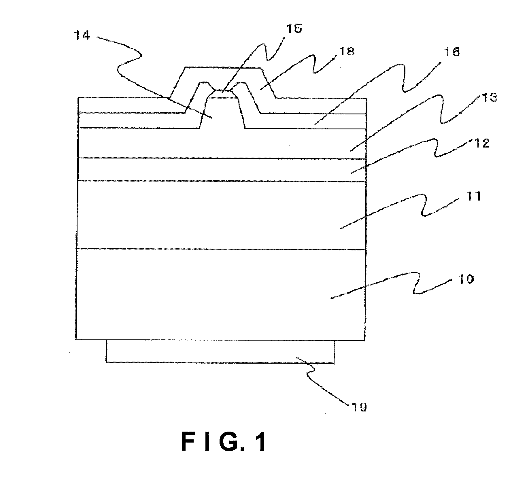
[0079]A semiconductor laser device of the present example includes, as shown in FIG. 1, a semiconductor layer of an n-side semiconductor layer 11, an active layer 12, and a p-side semiconductor layer 13 stacked in this order is formed on a GaN substrate 10 having a C-plane as a growth surface, and a ridge 14 is formed on the surface of the p-side semiconductor layer 13. A p-side electrode 15 is ohmically connected to the upper surface of the ridge 14. The electrode 15 has a flat portion 15a and sloped portions 15b. Each sloped portion 15b of the electrode is covered with the end portion 16a of the protective film and a pad electrode is electrically connected to the flat portion 15a of the electrode 15.

[0080]Further, although not shown, a dielectric film made of Al2O3 is formed on the cavity end surface of the semiconductor layer. Also, a p-side pad electrode 18 is formed to cover the electrode 15 and the protective film 16.

[0081]Such a semiconductor laser device can be formed accord...

example 2

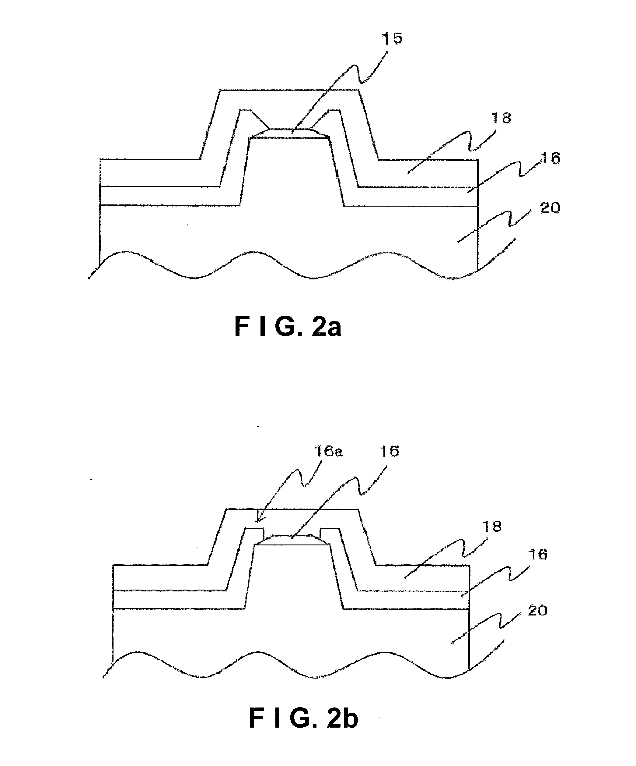
[0094]The semiconductor laser device of the present example is formed such that the third mask layer 23 is formed to cover the flat portion and a part of the sloped portion of the electrode in the manufacturing steps described in Example 1. Specifically, the width of the third mask layer 23 is about 14.0 μm and the thickness of the third mask layer is about 2.5 μm. Except as described above, the semiconductor laser device is manufactured in substantially the same manner as the semiconductor laser device of Example 1. Accordingly, as shown in FIG. 2b, a region covered by the tip end portion 16a of the protective film and a region connected to the p-side pad electrode are formed on each sloped portion of the electrode. Substantially the same effects as in Example 1 can also be obtained in this example.

example 3

[0095]The semiconductor laser device of the present example is formed such that the third mask layer 23 is formed to cover only the flat portion of the electrode in the manufacturing steps described in Example 1. The width of the third mask layer 23 is about 12.0 μm and the thickness of the third mask layer is about 2.5 μm. Except as described above, the semiconductor laser device is manufactured in substantially the same manner as the semiconductor laser device of Example 1. Accordingly, as shown in FIG. 2c, the tip end 16a of the protective film covers the sloped portions 15b of the electrode and a part of the flat portion 15a of the electrode. Effects substantially the same as that in Example 1 can also be obtained in this example.


PUM


Abstract

A semiconductor device includes a semiconductor layer stacked on a substrate, a stripe-shaped ridge formed on a surface of the semiconductor layer, and electrode formed on an upper surface of the ridge and a protective film disposed on each side of the ridge. The electrode includes a flat portion having a flat surface substantially parallel to the upper surface of the ridge and sloped portions on both sides of the flat portion with each of the sloped portions having a sloped surface that is sloped with respect to the upper surface of the ridge. The protective film covers a region from a side surface of the ridge to the sloped surface of the sloped portion of the electrode.

Description

CROSS-REFERENCE TO RELATED APPLICATIONS[0001]This application claims priority to Japanese Patent Application No. 2009-134281 filed on Jun. 3, 2009. The entire disclosure of Japanese Patent Application No. 2009-134281 is hereby incorporated herein by reference.BACKGROUND[0002]1. Technical Field[0003]The present invention relates to a semiconductor device and a method of manufacturing the semiconductor device, and particularly to a semiconductor device having a ridge and a method of manufacturing the semiconductor device.[0004]2. Related Art[0005]There has been proposed is a compound semiconductor device in which a stripe-shaped ridge is formed on a surface of a p-side semiconductor layer of a compound semiconductor device, and a part of an active layer below the ridge is designated as an optical waveguide region. In such a compound semiconductor device, generally, a stripe-shaped ridge is formed on a surface of a compound semiconductor layer stacked on a substrate, and an electrode i...

Claims


Application Information

Patent Timeline
IPC IPC(8): H01L29/06H01L21/28
CPCH01S5/0213H01S5/0218H01S5/22H01S5/0425H01S5/32341H01S2301/176H01S5/2205H01S5/04252H01S5/04254
Inventor MICHIUE, ATSUOKAWATA, YASUHIRO
Owner NICHIA CORP
Why Eureka
Try Eureka