Bootstrap Circuitry

a circuitry and bootstrap technology, applied in the field of bootstrap circuitry, can solve the problems of insufficient voltage of controller power supply capacitor derived from auxiliary power supply waste of power in an smps, and insufficient voltage of controller power supply capacitor to power the controller, so as to reduce power wastage and increase start-up time

Inactive Publication Date: 2010-12-09
CAMBRIDGE SEMICONDUCTOR LIMITED
View PDF12 Cites 111 Cited by
  • Summary
  • Abstract
  • Description
  • Claims
  • Application Information

AI Technical Summary

Benefits of technology

[0089]According to a fifth aspect of the present invention, there is provided a bootstrap circuit for a switched mode power supply, which may be similar to the second aspect but wherein the power switch is a field effect transistor, e.g., MOSFET, JFET, IGFET, etc. Thus, any combination of the optional features of the second aspect may apply to the fifth aspect, taking into account the use of a field effect transistor as the power switch. Current amplification may still occur using such a transistor, albeit on a different scale in comparison to when using a bipolar transistor as the power switch (Q1). Nevertheless, such a circuit may advantageously operate to reduce power wastage and/or increase start-up time.
[0090]Thus, the fifth aspect provides a bootstrap circuit for a switch mode power supply, the switch mode power supply for converting a voltage of an input power rail, the switch mode power supply comprising: a transformer having a primary winding coupled to r

Problems solved by technology

For example, such other condition may be a fault condition, this in embodiments resulting in a cessation of switching of the power switch.
More specifically, the voltage of charge on the controller power supply capacitor derived from the auxiliary power supply may be insufficient to power the controller if the voltage is less than that required to activate a power or voltage regulator internal to the controller.
Wasted power in an SMPS, which may otherwise be around 10 mW, is particularly disadvantageous in unloaded (or standby) conditi

Method used


Image

  • Bootstrap Circuitry
  • Bootstrap Circuitry
  • Bootstrap Circuitry

Examples


Embodiment Construction

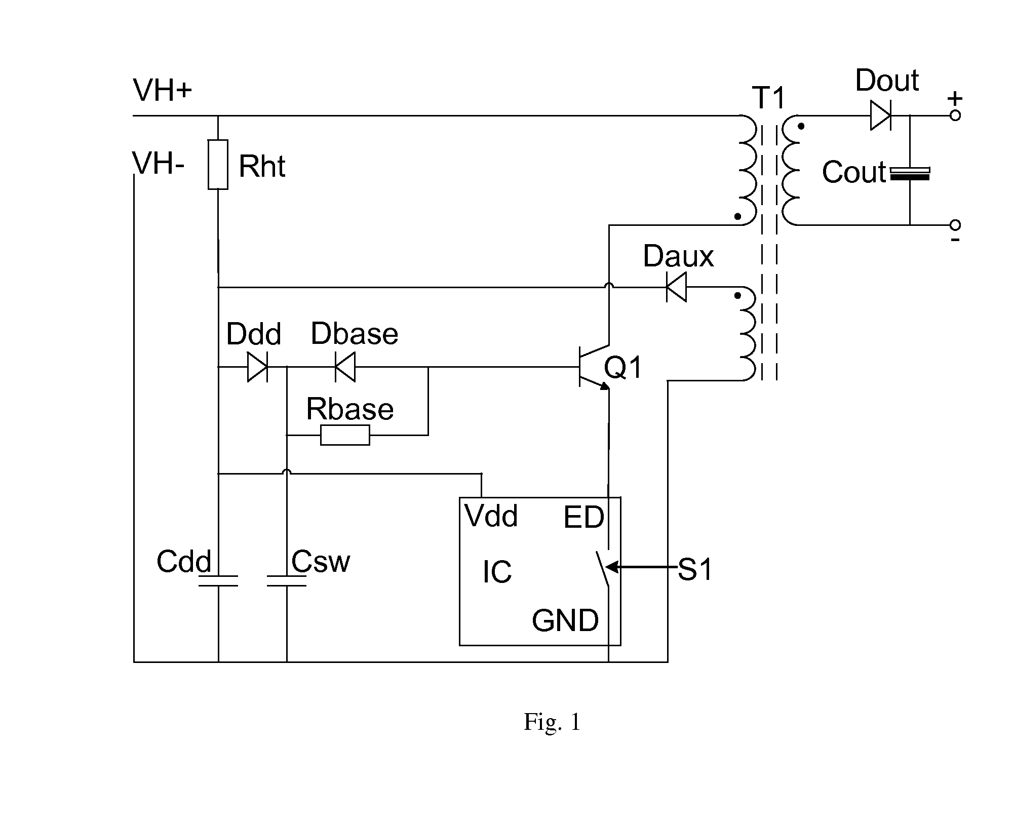
[0102]The proposed schemes are particularly applicable to an SMPS employing an emitter-(or source-) switched power transistor and merely less so to a base- (or gate-) driven arrangement.

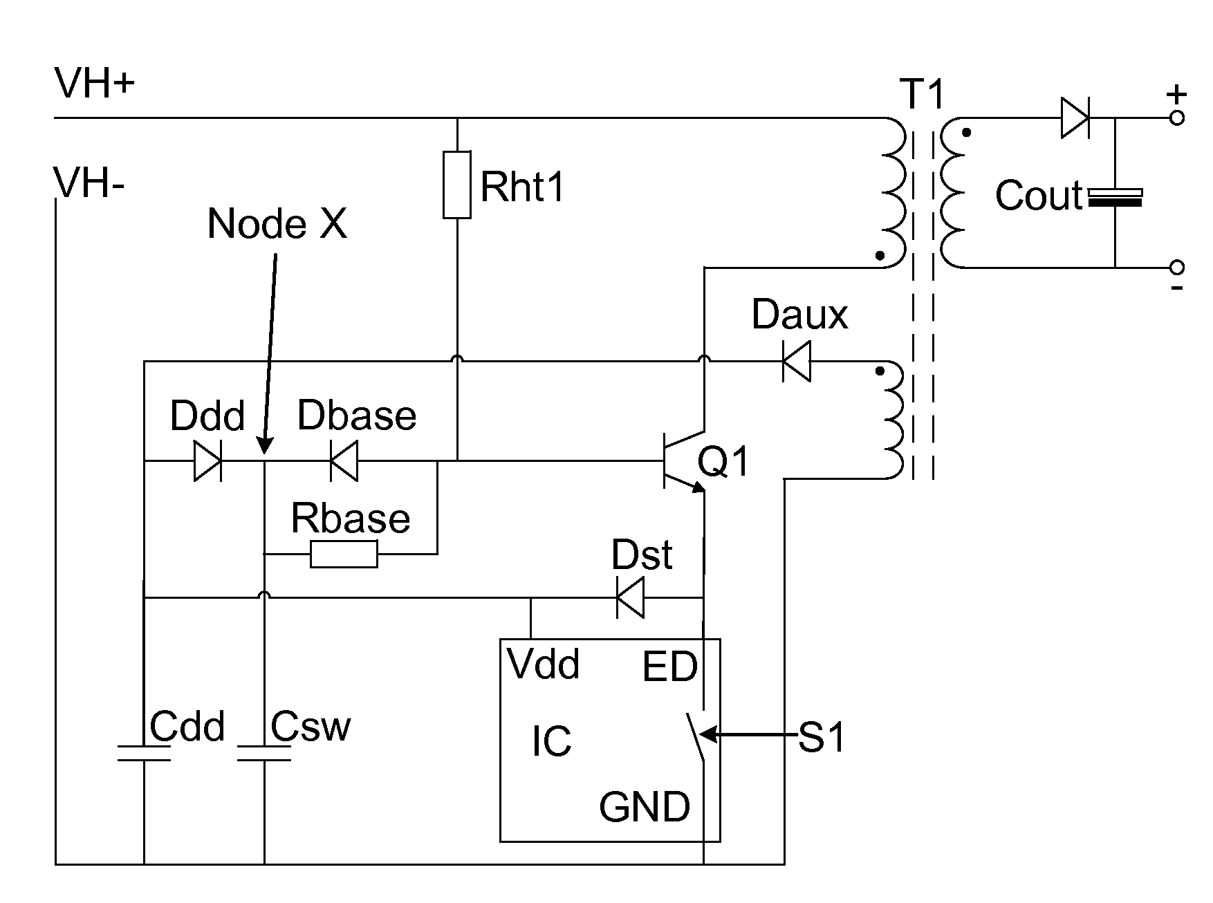
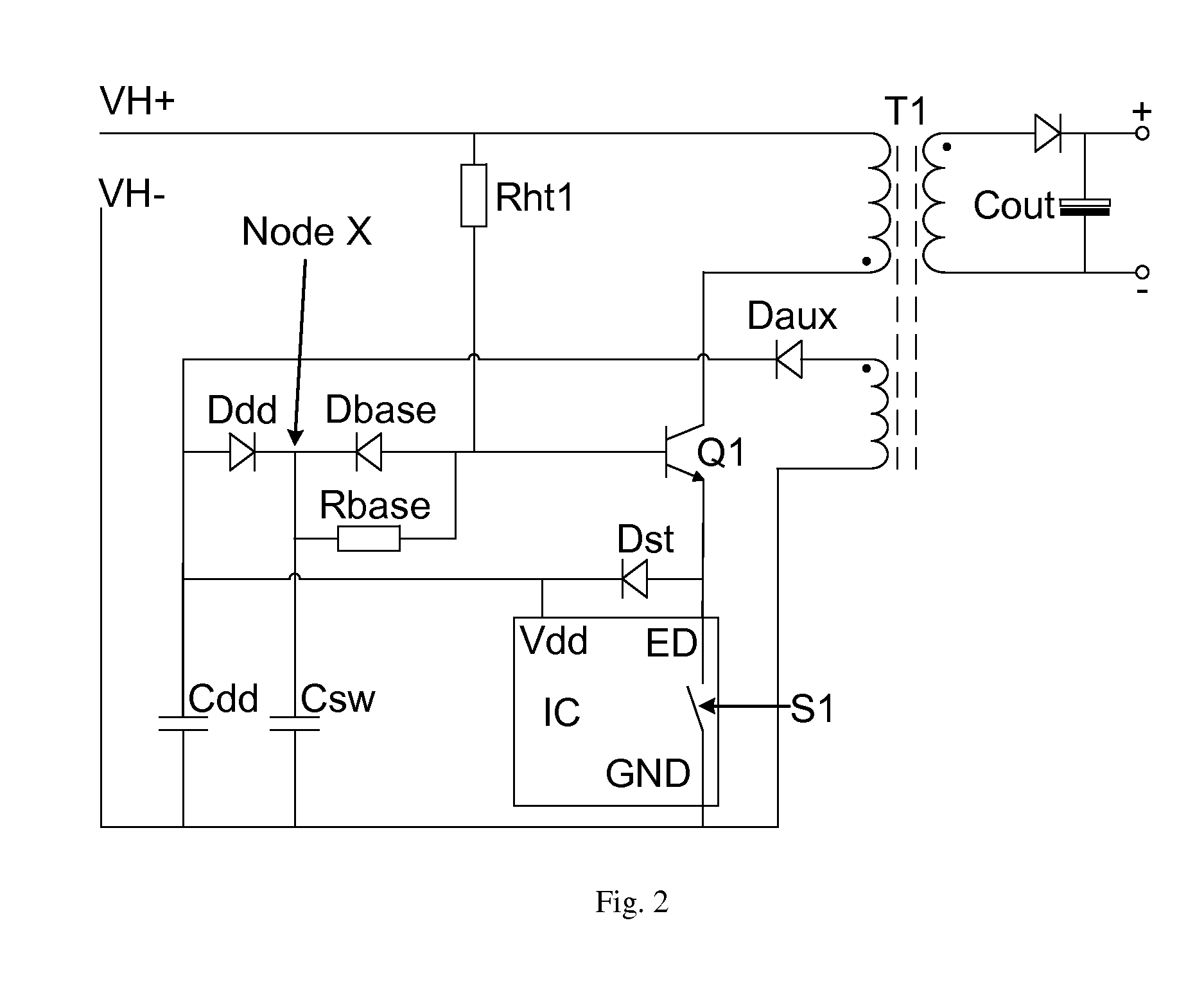
[0103]An embodiment of a bootstrap scheme employs the gain of a power transistor Q1 to provide an amplified start-up current to an SMPS controller (e.g. control IC), this allowing a very high-valued start-up resistor Rht1 to be used. This, and the prevention of such amplified Q1 start-up current from flowing after the start-up period, reduces the associated power loss. The scheme is illustrated below in the simplified circuit diagram of FIG. 2.

[0104]Embodiments may advantageously achieve either or both of the following:[0105]1) a fast start-up for a circuit (e.g. Switched-Mode Power Supply) with minimal power wastage; and / or[0106]2) a precise input voltage threshold for a circuit (e.g. Switched-mode Power Supply) to start up.

[0107]Furthermore, particular embodiments of configuring the start-up circui...


PUM


Abstract

This invention generally relates to a bootstrap circuit for a switch mode power supply, a controller for a switch mode voltage converter, a switch mode flyback converter comprising the bootstrap circuit, a switch mode forward converter comprising the bootstrap circuit, and a method of bootstrapping a switch mode power converter. The bootstrap circuit comprises: a current bleed impedance (Rht1) to bleed current from an input power supply (VH+); circuitry to deliver current from the input power supply (VH+) via the current bleed impedance (Rht1) to the base of a power switch (Q1) such that the power switch (Q1) is operable to amplify the current delivered from the internal power supply; a passive circuit (Dst) to provide the amplified current to a reservoir capacitor (Cdd); and the passive circuit element (Dst) further to substantially block reverse current flow from the supply input (Vdd) to the emitter of the power switch (Q1).

Description

RELATED APPLICATIONS[0001]The present invention claims priority from U.S. Provisional Patent Application No. 61 / 183,720, filed Jun. 3, 2009.FIELD OF THE INVENTION[0002]The invention generally relates to a method of bootstrapping a switch mode power converter, bootstrap circuits for a switch mode power supply, a controller for a switch mode voltage converter, and a switch mode voltage converter. In particular, the invention relates to a bootstrap circuit further comprising brownout protection circuitry.BACKGROUND TO THE INVENTION[0003]A schematic diagram of a Switched Mode Power Supply (SMPS) having an emitter-switched flyback topology is shown in FIG. 1. In a fully operational (‘normal’) state, the supply current for the controller integrated circuit (IC) is delivered to the Vdd terminal from an auxiliary (or bias) winding, via diode (Daux) and reservoir capacitor (Cdd). However, during the start-up (also referred to as ‘bootstrap’) phase, which occurs after initial switch-on and be...

Claims


Application Information

Patent Timeline
IPC IPC(8): H02M3/335
CPCH02M3/33507H03K17/567H03K17/107H02M2001/0096H02M1/088H02M1/0096
Inventor COULSON, DAVID
Owner CAMBRIDGE SEMICONDUCTOR LIMITED
Why Eureka
Try Eureka