

Non-volatile memory
a non-volatile memory and memory cell technology, applied in the field of semiconductor devices, can solve the problems of leakage current, affecting device reliability, and little sensitivity to defeat, and achieve the effect of improving device efficiency and memory cell integrity
- Summary
- Abstract
- Description
- Claims
- Application Information
AI Technical Summary
Benefits of technology
Problems solved by technology
Method used
Image

Examples
Embodiment Construction
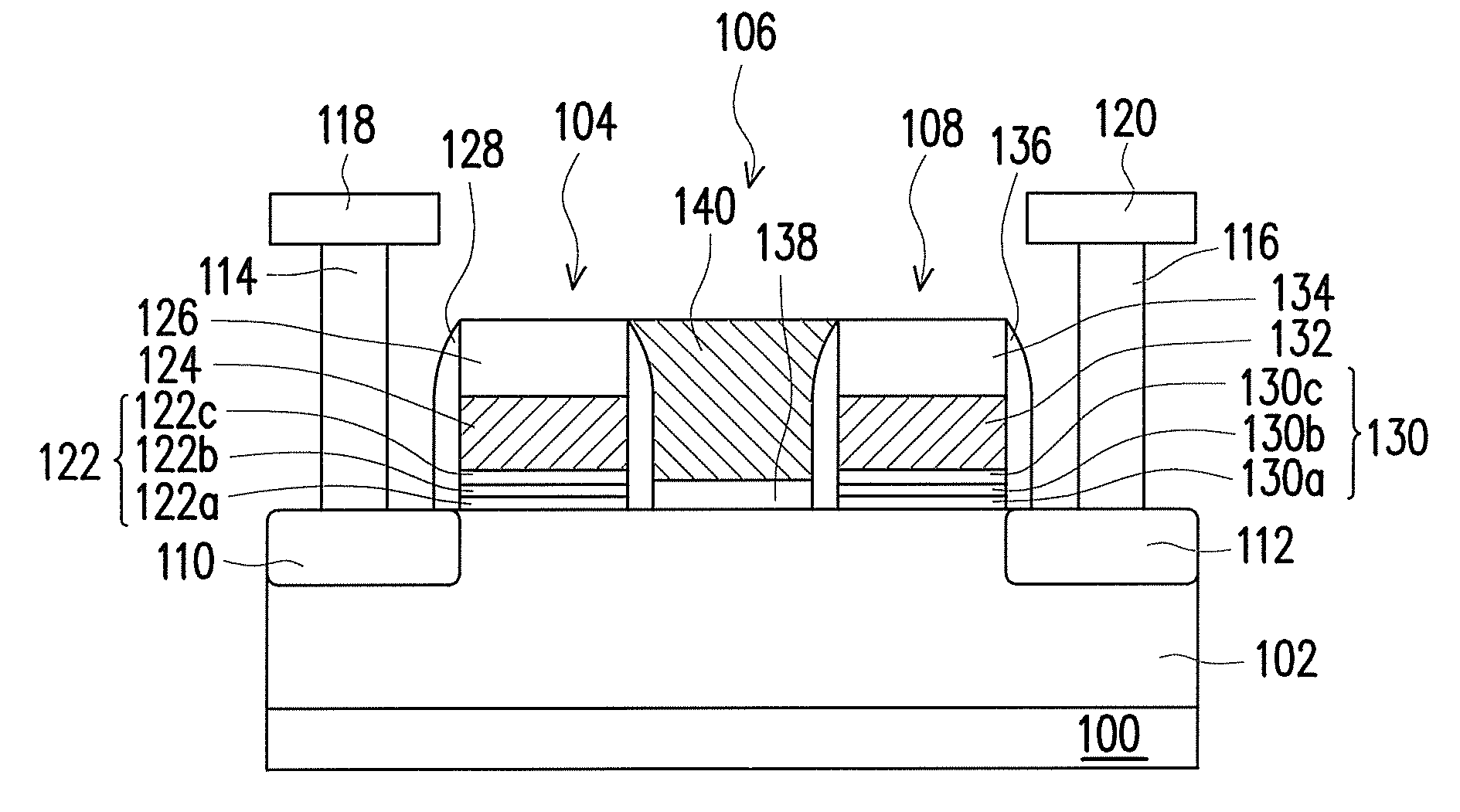
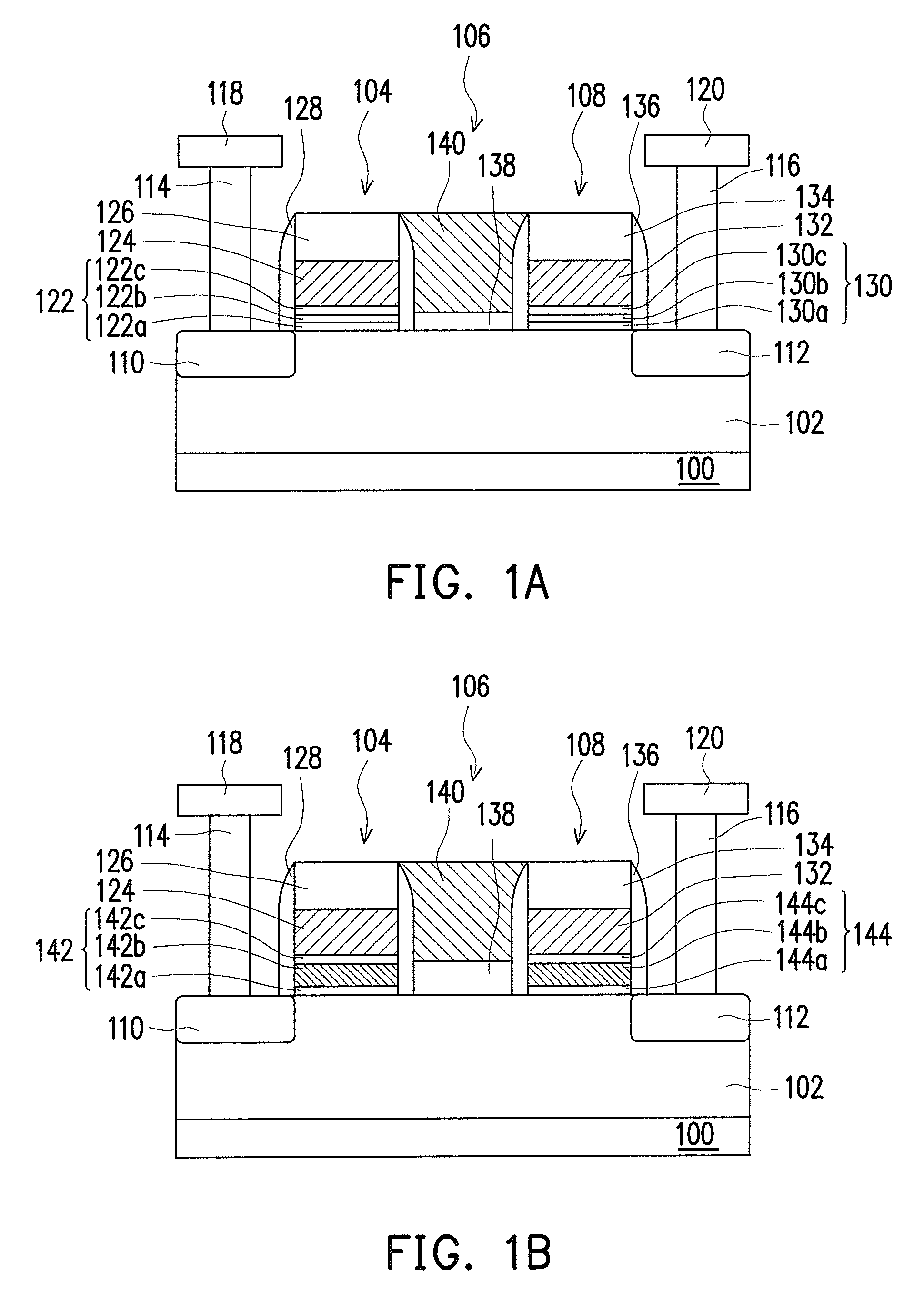
[0057]FIG. 1A is a cross-sectional diagram of a non-volatile memory unit according to one embodiment of the present invention.
[0058]Referring to FIG. 1A, the non-volatile memory unit of the present invention includes: a substrate 100, a well region 102, a memory cell 104, a select gate structure 106, a memory cell 108, a doped region 110, a doped region 112, a conductive plug 114, a conductive plug 116, a conductive wire 118 (bit line), and a conductive wire 120 (bit line).
[0059]The substrate 100 is, for example, silicon substrate. The substrate 100 can be a P-type substrate or an N-type substrate. The well region 102 is, for example, disposed in the substrate 100.
[0060]The doped region 110 and the doped region 112 are, for example, disposed in the substrate 100. The memory cell 104, the select gate structure 106 and the memory cell 108 are, for example, disposed on the substrate 100 between the doped region 110 and the doped region 112. The memory cell 104 is adjacent to the doped ...
PUM
 Abstract
Description
Claims
Application Information