

Optical modulator
a technology of optical modulator and electric line, applied in non-linear optics, instruments, optics, etc., can solve the problems of insufficient reduction of equivalent refractive index, ineffective use of gap portions, and inability to effectively solve gaps, etc., to improve optical modulation characteristics, reduce the length and reduce the number of electric lines of force
- Summary
- Abstract
- Description
- Claims
- Application Information
AI Technical Summary
Benefits of technology
Problems solved by technology
Method used
Image

Examples
first embodiment
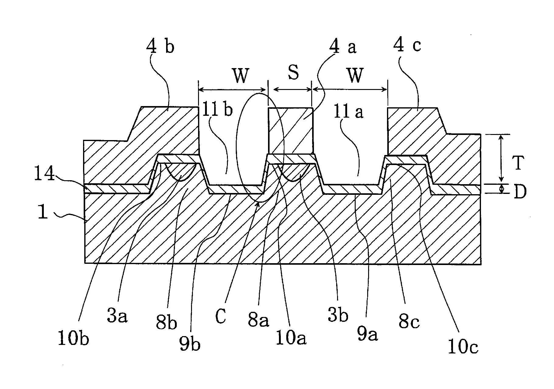
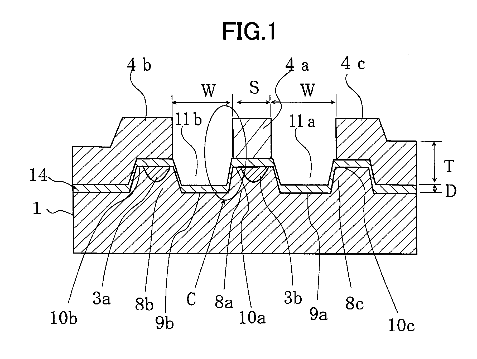
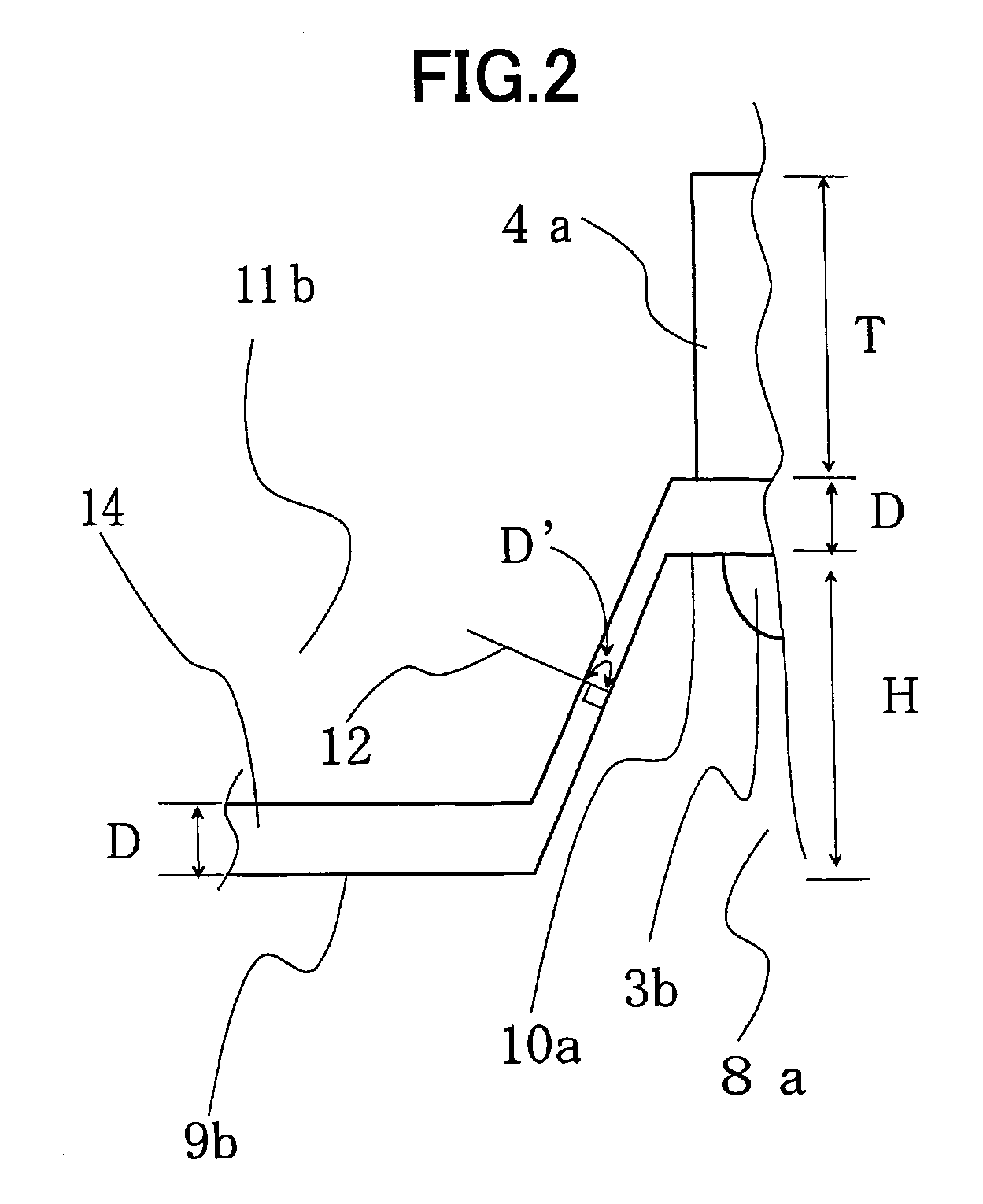
[0087]The optical modulator according to the first embodiment of the present invention has an SiO2 buffer layer 14. FIG. 1 is a sectional view schematically showing the optical modulator which is manufactured by controlling the deposition of the SiO2 buffer layer 14. FIG. 2 is an enlarged view of the area C in FIG. 1. In this embodiment, as can be seen from FIG. 1 or FIG. 2, the thickness D′ of the SiO2 buffer layer 14 on the side surface of the ridge portion 8a is less than the thickness D of the SiO2 buffer layer 14 on the bottom surfaces 9a, 9b between the ridge portions or on the top parts 10a to 10c of the ridge portions. As in the case of FIG. 19, the Si conducting layer for suppressing the temperature drift is omitted in the first embodiment and in the second embodiment to avoid the tedious explanation.
[0088]Although the thickness of the SiO2 buffer layer 14 on the bottom surfaces 9a, 9b between the ridge portions and the thickness of the SiO2 buffer layer 14 on the top parts...
second embodiment
[0098]The optical modulator according to the second embodiment of the present invention has an SiO2 buffer layer 15. FIG. 8 is a sectional view schematically showing the optical modulator which is manufactured by controlling the deposition of the SiO2 buffer layer 15. FIG. 9 is an enlarged view of the area E in FIG. 8. The thickness of the SiO2 buffer layer 15 on the bottom surface 9a between the ridge portions 8a and 8c (and on the bottom surface 9b between the ridge portions 8a and 8b) is different from the thickness of the SiO2 buffer layer 15 on the top part 10a (and 10b, 10c) of the ridge portions. The thickness of the SiO2 buffer layer on the side surface of the ridge portion 8a (and 8b and 8c) is less than a larger one of the thickness of the SiO2 buffer layer 15 on the bottom surface 9a between the ridge portions 8a and 8c (and on the bottom surface 9b between the ridge portions 8a and 8b) and the thickness of the SiO2 buffer layer 15 on the top part 10a (and 10b, 10c) of th...
third embodiment
[0101]The optical modulator according to the third embodiment of the present invention has an Si conducting layer 16 for suppressing the temperature drift. FIG. 10 is a sectional view schematically showing the optical modulator which is manufactured by controlling the deposition of the SiO2 buffer layer 14 and the Si conducting layer 16. FIG. 11 is an enlarged view of the area F shown in FIG. 10. These figures are to more fully explain the first embodiment of the present invention shown in FIGS. 1 and 2, where the explanation of the Si conducting layer 16 for suppressing the temperature drift is not omitted, although the Si conducting layer 16 is omitted only for simplicity in FIGS. 1 and 2.
[0102]As mentioned above, a relative permittivity of the Si conducting layer 16 is 11 to 13, which is much larger than a relative permittivity of 4 to 6 of the SiO2 buffer layer 14. For example, the Si conducting layer 16 with a thickness of 0.2 μm corresponds to the SiO2 buffer layer 14 with a t...
PUM
| Property | Measurement | Unit |
|---|---|---|
| width | aaaaa | aaaaa |
| width | aaaaa | aaaaa |
| thickness | aaaaa | aaaaa |
Abstract
Description
Claims
Application Information