Photovoltaic assembly comprising an optically active glass ceramic
a technology of optical active glass and photovoltaic assembly, applied in the field of solar cells, can solve the problems of mechanical brittleness of many phosphors, sometimes even water-soluble or hygroscopi
- Summary
- Abstract
- Description
- Claims
- Application Information
AI Technical Summary
Benefits of technology
Problems solved by technology
Method used
Image
Examples
Embodiment Construction
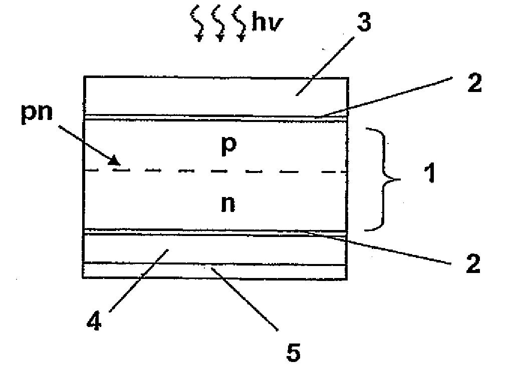
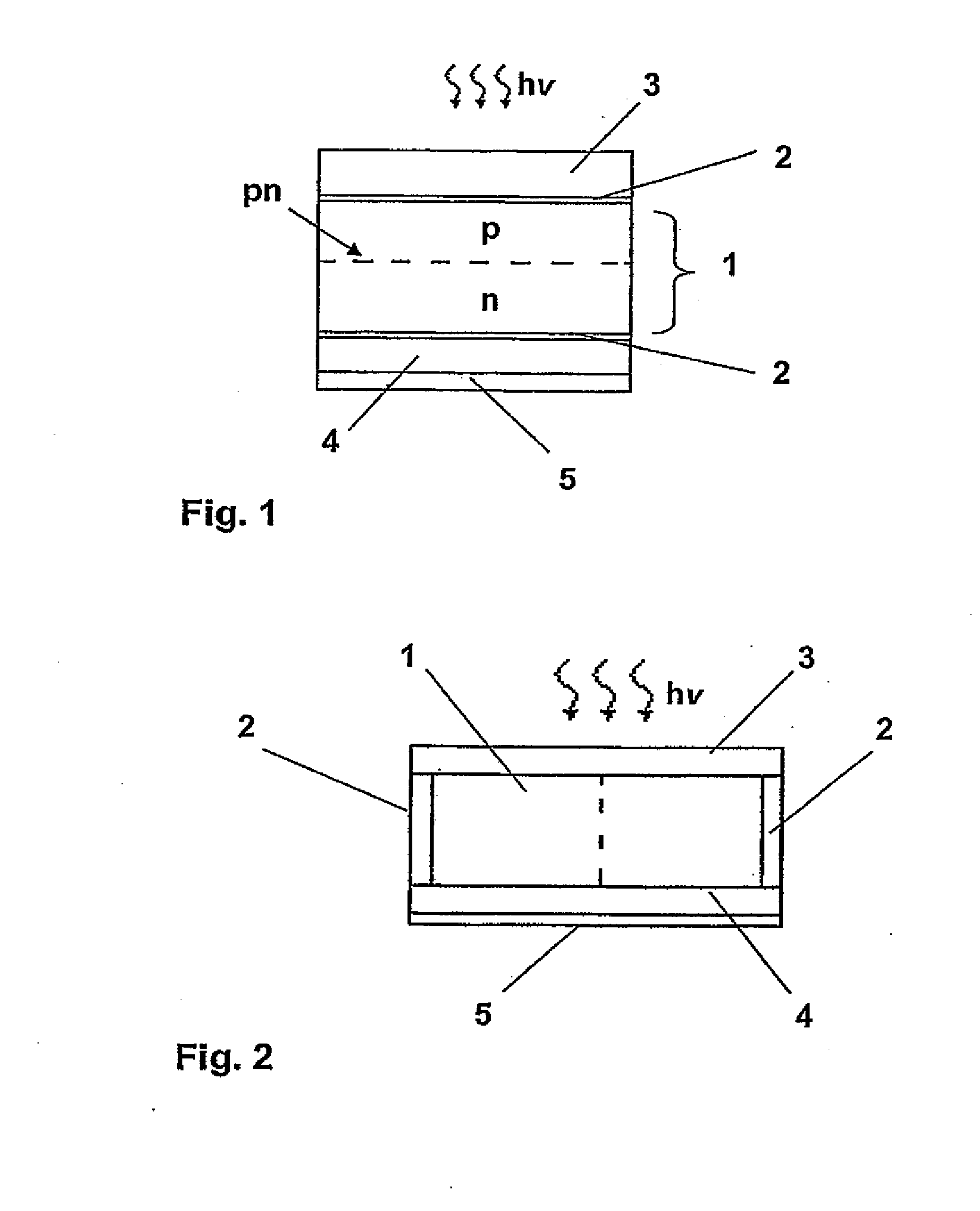
[0042]FIG. 1 shows a photovoltaic layer region (1), which is contacted via two electrode assemblies situated in the layers. For example, the photovoltaic layer region 1 can be implemented by one p-doped semiconductor layer and one n-doped semiconductor layer. A space charge region is implemented at the boundary surface between the p-doped layer and the n-doped layer, the p-n junction, and a potential difference arises over the space charge region, which can be tapped at the electrodes in the form of an electrical voltage.
[0043]Photons hv having a minimum energy Emin may be absorbed in the space charge region, one electron from the valence band being raised into the conduction band of the semiconductor. In this way, a freely moving electron arises in the conduction band and a freely moving hole arises in the valence band. One electron-hole pair accordingly arises per absorbed photon. This pair is spatially separated by the potential difference implemented at the p-n junction. The fre...
PUM
 Abstract
Description
Claims
Application Information

