Configurations and methods for manufacturing devices with trench-oxide-nano-tube super-junctions

a manufacturing method and super-junction technology, applied in the direction of semiconductor devices, basic electric elements, electrical appliances, etc., can solve the problems of limiting reducing the efficiency of super-junction semiconductor devices, and reducing the practical usefulness of these devices, so as to reduce the concentration of boron doping, improve the practical usefulness of super-junction semiconductor devices, and reduce the production cost

Active Publication Date: 2010-12-16
ALPHA & OMEGA SEMICON INC
View PDF4 Cites 77 Cited by
  • Summary
  • Abstract
  • Description
  • Claims
  • Application Information

AI Technical Summary

Benefits of technology

[0013]Another aspect of the present invention is to provide a new and improved device structure and manufacturing method with a super junction structure by growing a thin single layer N− epitaxial layer (0.1-1.0 micron thickness range) partially filling the trenches, and filling the rest of the deep trenches with dielectric/oxide thus resolving the problems of high production cost of the superjunction devices due to slow epitaxial growth in the deep trenches. Additionally, a lowly doped N type epitaxial layer may be grown after the N-epi, substantially filling the trench, before filling the rest of the deep trenches with dielectric/oxide, which may make it easier to fill the trench with oxide.
[0014]Another aspect of the present invention is to provide a new and improved device structure and manufacturing method with a super junction structure by forming a very thin N-type Nano-Tube layer next to and charge balanced with a wider P-type region; by way of example, having a 3 times wider P-type region results in 3 times lower Boron doping concentration than N-type doping concentration in the N-type Nano-Tube region. Thus only limited Boron diffusion is allowed into the N type Nano-Tube region which can be compensated with extra Arsenic charge. Heavy N type dopants such as Arsenic or Antimony for the N-type Nano-Tube region do not move much and so will not diffuse significantly into the P-type region. Therefore, the problems caused by inter diffusion of N and P impurities at high temperature are resolved.
[0015]Another aspect of the present invention is to provide a new and improved device structure and manufacturing method with a super junction structure by increasing the width of the trench region at the boundary of a first device, for example a MOSFET device and a second device such as a Schottky diode, with the large trench region substantially filled with dielectric material—as opposed to active cells which are substantially filled with silicon and the rest with silicon oxide (oxide, or SiO2). Different devices can therefore be more conveniently integrated on a same silicon chip.
[001

Problems solved by technology

Even though there have been many patented disclosures and published technical papers related to semiconductor devices with vertical super junction structure to achieve improved electrical characteristics, those who are involved in the fields of designing and manufacturing the super-junction semiconductor devices are still confronted with technical difficulties and manufacturability limitations.
However, the configurations and operational characteristics of the super junction devices as disclosed in these patented and published disclosures still encounter technical limitations thus restricting the practical usefulness of these devices.
The difficulties and limitations of the convention

Method used


Image

  • Configurations and methods for manufacturing devices with trench-oxide-nano-tube super-junctions
  • Configurations and methods for manufacturing devices with trench-oxide-nano-tube super-junctions
  • Configurations and methods for manufacturing devices with trench-oxide-nano-tube super-junctions

Examples


Embodiment Construction

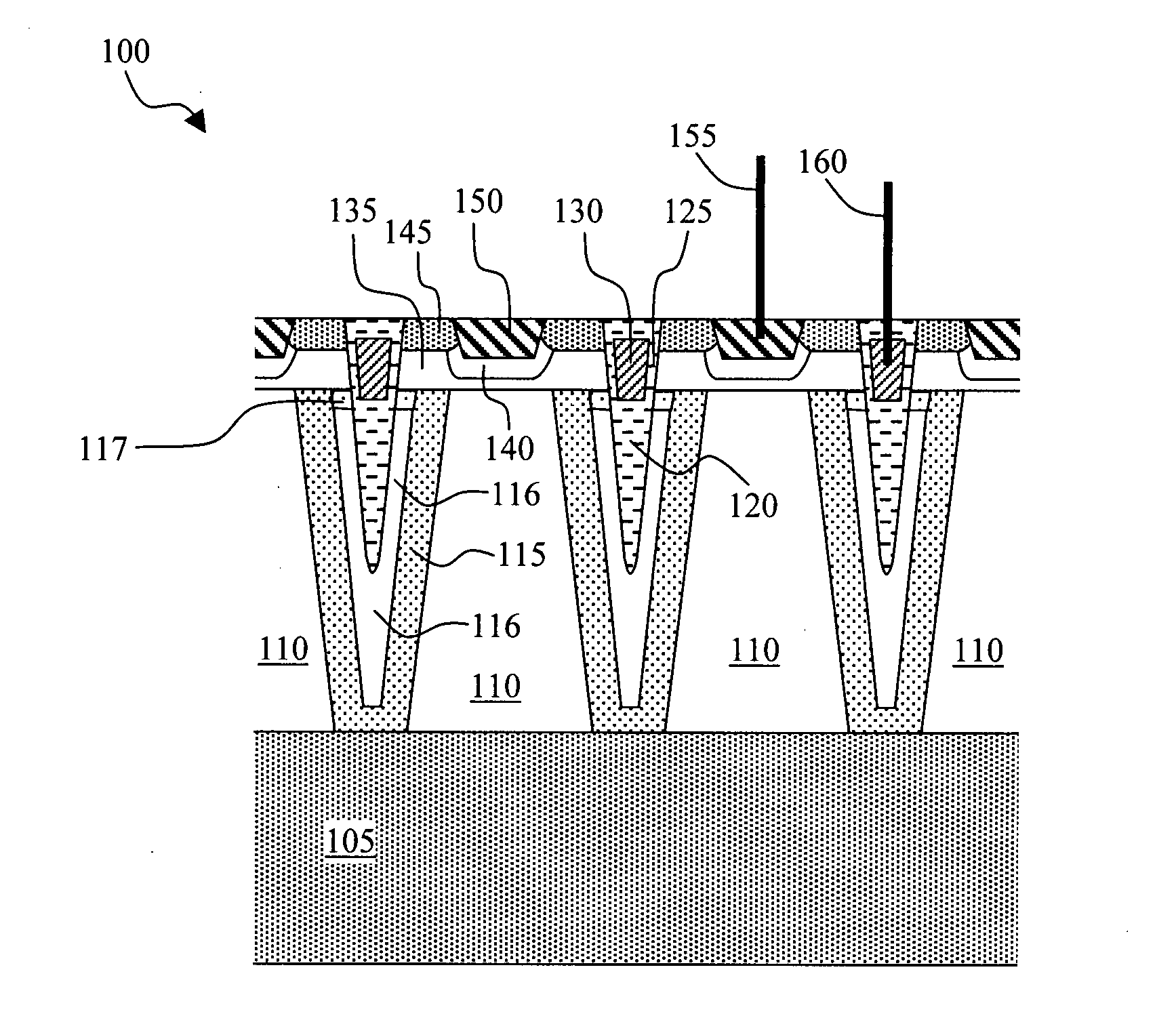
[0035]FIG. 2 shows a cross sectional view of a trench nano-tube metal oxide semiconductor field effect transistor (MOSFET) device 100 of this invention. The MOSFET cells are formed in a P-type epitaxial layer 110 supported on an N+ substrate 105. A plurality of trench nano tubes 115 and a plurality of trenches are formed in the epitaxial layer 110. The trenches are formed with sidewalls having a slightly tilted angle to form a tapered trench. By way of example the walls may be slightly tilted at 87-89 degrees. Each of the trench sidewalls is covered with an N+ epitaxial layer 115. An additional lowly doped P− epitaxial layer 116 is grown over the N+ epitaxial layer 115. Because of the remaining trench width and the tilted angle of the trench, the sidewalls of the P− epitaxial layer 116 converge towards the bottom and substantially fill the bottom portion of the trench. The remaining central portion of the trenches is filled with a dielectric such as silicon oxide 120. The MOSFET dev...


PUM


Abstract

This invention discloses semiconductor power device disposed on a semiconductor substrate of a first conductivity type. The semiconductor substrate supports an epitaxial layer of a second conductivity type thereon wherein the semiconductor power device is supported on a super-junction structure. The super-junction structure comprises a plurality of trenches opened from a top surface in the epitaxial layer; wherein each of the trenches having trench sidewalls covered with a first epitaxial layer of the first conductivity type to counter charge the epitaxial layer of the second conductivity type. A second epitaxial layer may be grown over the first epitaxial layer. Each of the trenches is filled with a non-doped dielectric material in a remaining trench gap space. Each of the trench sidewalls is opened with a tilted angle to form converging U-shaped trenches.

Description

[0001]This application is a Continuation-in-Part (CIP) of U.S. application Ser. No. 12 / 484,166 and 12 / 484,170, both filed Jun. 12, 2009 and the disclosures made in these two applications are hereby incorporated by reference.BACKGROUND OF THE INVENTION[0002]1. Field of the Invention[0003]The invention relates generally to the semiconductor power devices. More particularly, this invention relates to configurations and methods implemented with trench nano-tubes with trench sidewalls covered with doped epitaxial layer and then filled with insulative material for manufacturing flexibly scalable charge balanced semiconductor power devices with simplified manufacturing processes and achieving improved breakdown voltage and significantly reduced resistance.[0004]2. Description of the Prior Art[0005]Even though there have been many patented disclosures and published technical papers related to semiconductor devices with vertical super junction structure to achieve improved electrical charact...

Claims


Application Information

Patent Timeline
IPC IPC(8): H01L29/78H01L21/336H01L21/762
CPCH01L29/0661H01L29/66348H01L29/7397H01L29/0634H01L29/7813
Inventor YILMAZ, HAMZABOBDE, MADHURLEE, YEEHENGGUAN, LINGPENGWANG, XIAOBINCHEN, JOHNBHALLA, ANUP
Owner ALPHA & OMEGA SEMICON INC
Why Eureka
Try Eureka