Semiconductor device

Inactive Publication Date: 2010-12-16
RENESAS ELECTRONICS CORP
View PDF5 Cites 4 Cited by
  • Summary
  • Abstract
  • Description
  • Claims
  • Application Information

AI Technical Summary

Benefits of technology

[0018]According to the present invention, the wiring length between the system GND and the address driver IC can be reduced and thus the wiring impedance can be reduced. It is thus

Problems solved by technology

Such fluctuation in the VSS2 potential leads to logic malfunction of the high-voltage output part 10.
Moreover, the fluctuation in the VSS2 potential also affects the VSS1 potential connected to the VSS2 through the resistor, which leads to malfunction of the low-voltage logic part 11.
However, the drive current of the PD

Method used


Image

  • Semiconductor device
  • Semiconductor device
  • Semiconductor device

Examples


Example

[0028]The invention will be now described herein with reference to illustrative embodiments. Those skilled in the art will recognize that many alternative embodiments can be accomplished using the teachings of the present invention and that the invention is not limited to the embodiments illustrated for explanatory purposed.

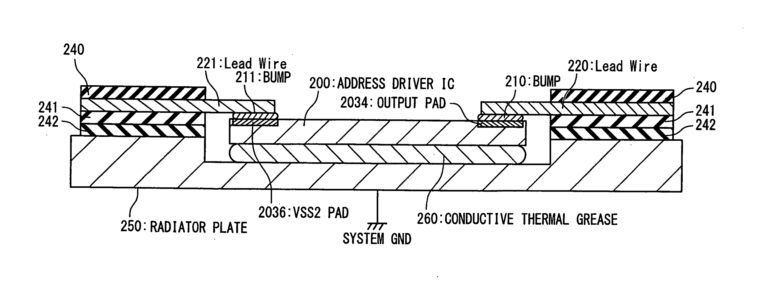
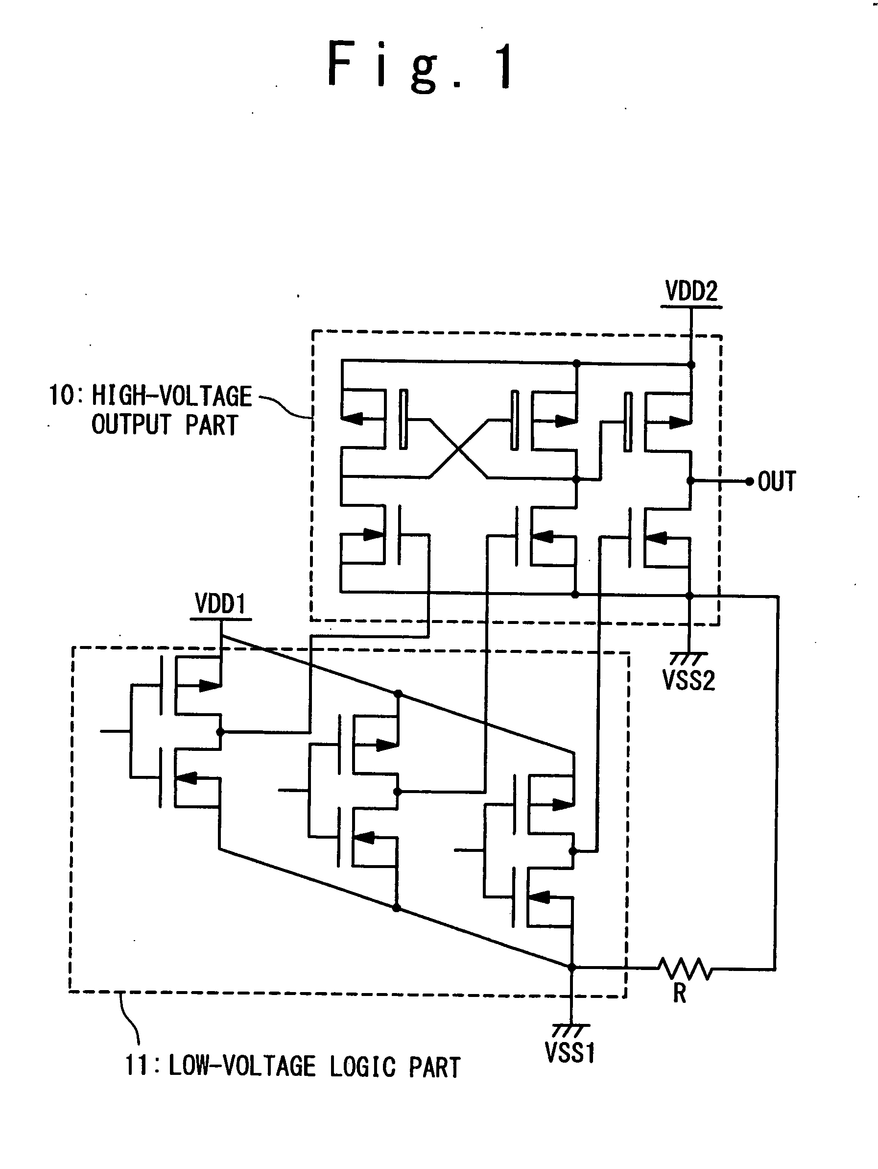
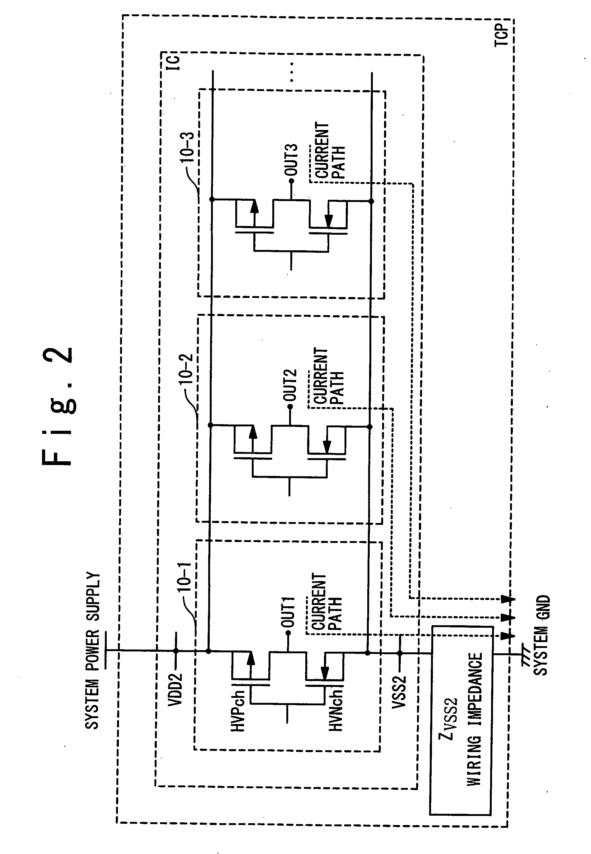
[0029]FIG. 4 is a plan view showing a configuration of a semiconductor device in an embodiment of the present invention. An address driver IC 200 (PDP address driver IC) is provided with a plurality of output cells 200-1. Each of the output cells 200-1 is provided with a high-voltage output part 2031 and a low-voltage logic part 2038. The high-voltage output part 2031 of the present embodiment is provided with a high-voltage P-channel MOSFET (Metal Oxide Semiconductor Field Effect Transistor) (hereinafter referred to as a HVPch), a high-voltage N-channel MOSFET (hereinafter referred to as a HVNch), and a contact hole 2037. Furthermore, the address driver IC 200 i...


PUM


Abstract

A semiconductor device has: a radiator plate that is maintained at a predetermined potential; an SOI (Silicon On Insulator) chip mounted on the radiator plate; and thermal grease applied to an interface between the radiator plate and the SOI chip. The SOI chip has: a first silicon substrate forming a circuit element part; a second silicon substrate facing the radiator plate; and an insulating film formed between the first silicon substrate and the second silicon substrate. The first silicon substrate and the second silicon substrate are electrically connected to each other. The thermal grease is conductive and electrically connects the second silicon substrate and the radiator plate.

Description

INCORPORATION BY REFERENCE[0001]This application is based upon and claims the benefit of priority from Japanese patent application No. 2009-142806, filed on Jun. 15, 2009, the disclosure of which is incorporated herein in its entirety by reference.BACKGROUND OF THE INVENTION[0002]1. Field of the Invention[0003]The present invention relates to a semiconductor device having a PDP (Plasma Display Panel) address driver IC.[0004]2. Description of Related Art[0005]A PDP driver IC (Integrated Circuit) includes a scan driver IC for driving scanning lines and an address driver IC for driving data lines. The address driver IC is provided with a low-voltage logic part and a high-voltage output part. FIG. 1 is a diagram showing a configuration example of an output cell of the address driver IC. A single output cell has the high-voltage output part 10 and the low-voltage logic part 11, and many output cells are integrated on a chip of the address driver IC.[0006]The low-voltage logic part 11 inc...

Claims


Application Information

Patent Timeline
IPC IPC(8): H01L23/48H01L21/822H01L23/12H01L23/36H01L27/04
CPCG09G3/296G09G2330/02H01L21/50H01L23/3735H01L23/3737H01L2924/3011H01L2224/73253H01L2924/13091H01L2924/00
Inventor KOBAYASHI, NOBUYUKI
Owner RENESAS ELECTRONICS CORP
Why Eureka
Try Eureka