Method for shielding a substrate from electromagnetic interference

a technology of electromagnetic interference and shielding material, which is applied in the direction of shielding materials, instruments, non-metal conductors, etc., can solve the problems of low conductivity of current state of the art compositions, achieve high electrical conductivity and electromagnetic shielding effectiveness, improve lightning strike protection and emi shielding properties, and reduce the amount of grounding wires and labor.

Inactive Publication Date: 2010-12-16
LORD CORP
View PDF85 Cites 32 Cited by
  • Summary
  • Abstract
  • Description
  • Claims
  • Application Information

AI Technical Summary

Benefits of technology

[0018]Because of the heterogeneous structure formed, the EMI shielding composition is able to induce a percolated network of conductive particles at particle concentrations considerable below that of traditional compositions that possess homogenous structures comprised of particles uniformly situated throughout the polymer matrix. Moreover, the heterogeneous structure formed during curing permits the sintering of particles thereby eliminating contact resistance between particles and in turn leading to dramatic improvements in thermal and electrical conductivity. Moreover, the continuous pathway of sintered metal permits carrying of substantial amounts of heat and electrical current which may be encountered in heat intensive or electric field intensive applications. The combination lower filler loading and related self-assembling of continuous pathways permits EMI materials that are lighter weight, easier to process, and have more resin available for improved wetting and adhesion to substrates.
[0030]In a further aspect of the present invention, the highly conductive, self-assembling adhesive or composite possessing exceptionally high electrical conductivity and electromagnetic shielding effectiveness at reduced filler loadings is applied to a substrate in a particular pattern of interconnecting traces of known thickness and aperture size to create a electromagnetic interference (EMI) shield / filter.

Problems solved by technology

Current state of the art compositions often lack high conductivity combined with such properties as light weight, dispensability, and adhesion, which are often required for robust EMI shielding applications.

Method used


Image

  • Method for shielding a substrate from electromagnetic interference
  • Method for shielding a substrate from electromagnetic interference

Examples


example 1

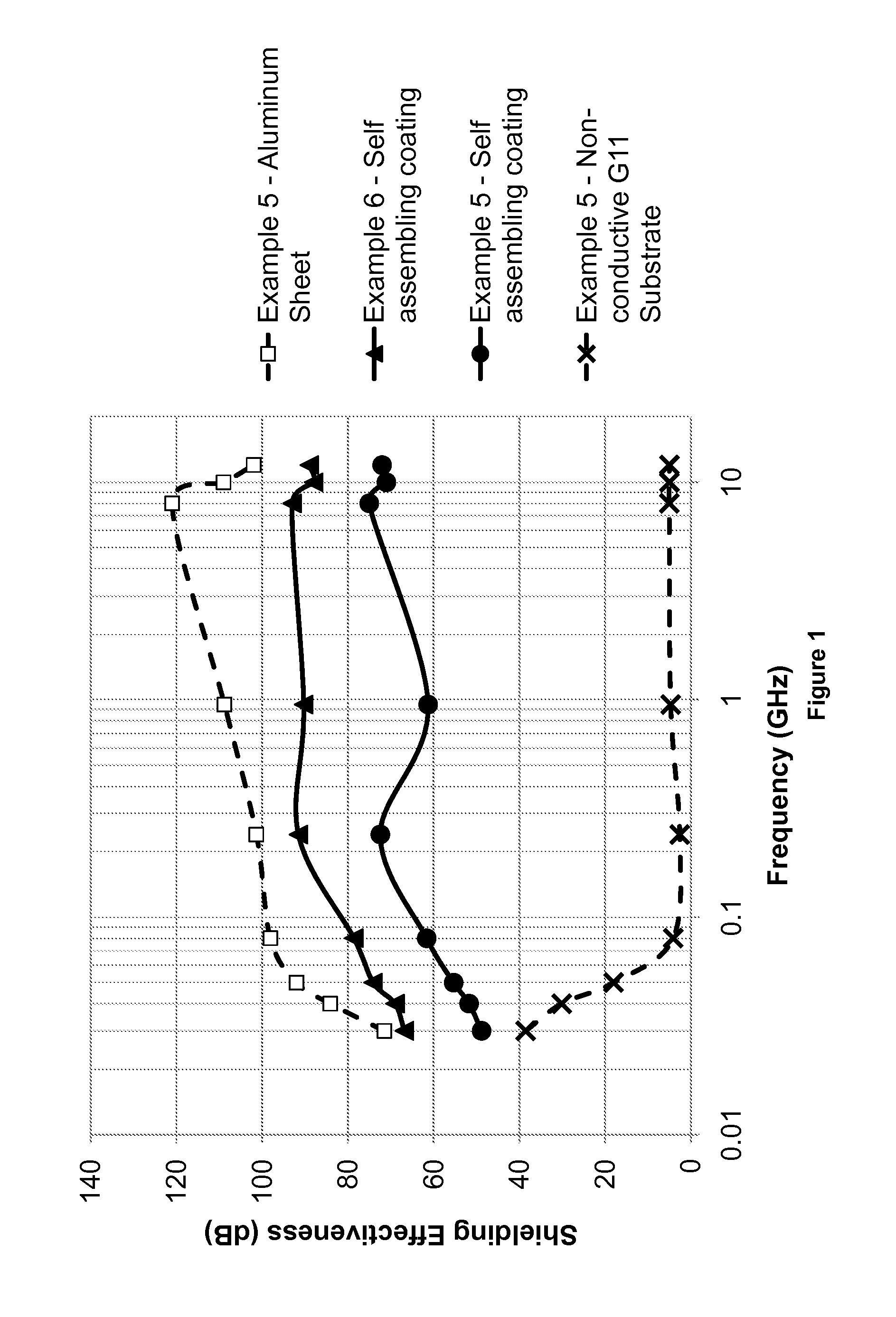
[0085]A conventional conductive particle-filled adhesive not of the present invention was prepared and tested for comparison purposes. The material contained 12.7 wt % DGEBF, 1.5 wt % diethylenetriamine and 85.8 wt % (40% by volume) silver flake type A described prior. The components were mixed until uniform in a Hauschild DAC 150 FV mixer. The material was molded into 40 mil thick disks to mimic a form-in-place gasket or adhesive. The mold was then cured at 160° C. for 1 hour. The resulting material exhibited a typical homogeneous morphology in which the filler was uniformly situated throughout the polymer matrix. The sheet resistance (Ω / square) was too high to be measured by a Keithly 580 multimeter equipped with a Bridge Technology SRM 4 point probe head. The shielding effectiveness (SE) averaged 18 decibels at frequencies of 2.6 GHz to 18 GHz as tested by Method I described prior.

example 2

[0086]A self-assembling adhesive of the present invention was prepared using the following formulation: 27.8 wt % DGEBF, 10.7 wt % amine adduct curative, and 61.5 wt % (15% by volume) silver flake type A. The material was molded, cured and tested according to the procedures in Example 1. The sheet resistance measured less than 0.001 Ω / square and the SE averaged 105 decibels. In comparison to Example 1, the self-assembling adhesive material in this example exhibited far superior SE at a lower concentration of conductive particles.

example 3

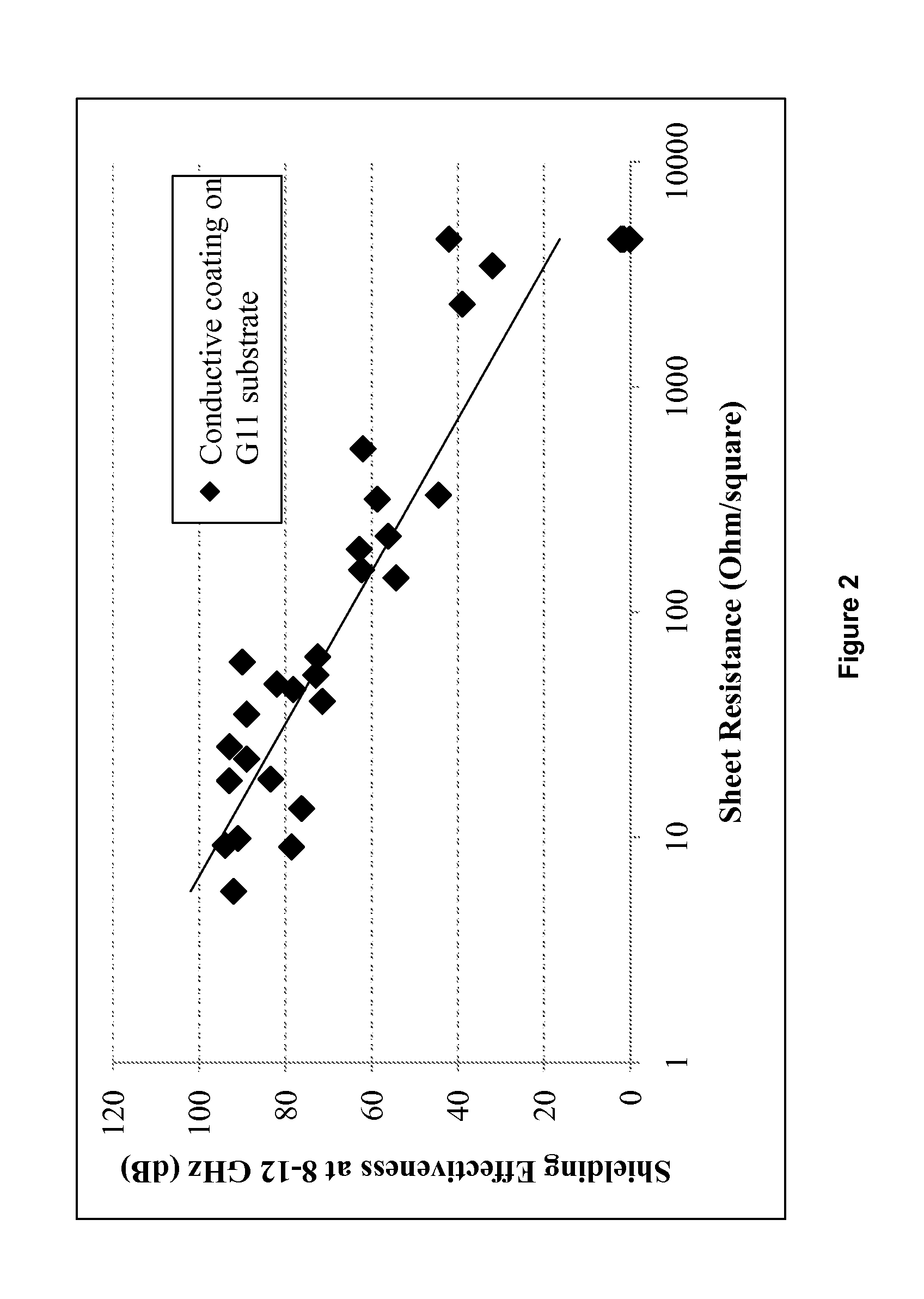
[0087]A self-assembling adhesive film of the present invention was prepared using 25.3 wt % DGEBF, 9.7 wt % amine adduct curative, and 65.0 wt % (17% by volume) silver flake type A. The components were mixed until uniform in a Hauschild DAC 150 FV mixer. Using a drawdown bar, a 1.5 mil thick film of the material was cast directly onto a non-conductive substrate of 0.125″ thick G11 epoxy board. The coated substrate was then cured at 160° C. for 1 hour. The sheet resistance of the cured film was 0.05 Ω / square. The SE averaged 72 decibels at frequencies of 8 GHz to 12 GHz as tested by Method I.


PUM

PropertyMeasurementUnit
shielding effectivenessaaaaaaaaaa
sizesaaaaaaaaaa

Abstract

A method for shielding a substrate from electromagnetic interference is provided including providing an electromagnetic interference (EMI) shielding composition to the substrate. The EMI shielding composition comprises a reactive organic compound and a conductive filler that, during the cure of the organic compound, is capable of self-assembling into a heterogeneous structure comprised of a continuous, three-dimensional network of metal situated among (continuous or semi-continuous) polymer rich domains. The resulting composition has exceptionally high thermal and electrical conductivity.

Description

CROSS-REFERENCE TO RELATED APPLICATIONS[0001]The present application claims priority under 35 U.S.C. §119(e) from U.S. Provisional Patent Application Ser. No. 61 / 186,492 filed Jun. 12, 2009, entitled “ELECTROMAGNETIC SHIELDING MATERIALS”, and U.S. Provisional Patent Application Ser. No. 61 / 186,415 filed Jun. 12, 2009, entitled “CURABLE CONDUCTIVE MATERIAL FOR LIGHTNING STRIKE PROTECTION”, the disclosures of which are incorporated herein by reference.FIELD OF THE INVENTION[0002]The present invention relates to electrically conductive polymeric coatings. More particularly, the present invention relates to electrically conductive compositions used as electromagnetic interference shielding coatings.BACKGROUND OF THE INVENTION[0003]Electromagnetic interference (EMI) is a common issue encountered in electronics communications. Foreign radiation is well known to induce undesirable currents in electronic components, thereby disrupting the normal operations. This issue is of particular conce...

Claims


Application Information

Patent Timeline
Patent Type & Authority Applications(United States)
IPC IPC(8): G01R27/08H01B1/12B05D5/12H05K3/00C09D7/62
CPCC09D7/62C09D5/24H05K9/0083C08G59/245C09D7/70C09D163/00C08K9/04C08G59/58H05K9/0079B05D1/02C08L63/00C09D7/40H01B1/22
Inventor FORNES, TIMOTHY D.
Owner LORD CORP
Why Eureka
Try Eureka