Enhancing NAND flash floating gate performance

a floating gate and nand flash technology, applied in the direction of semiconductor devices, basic electric elements, electrical equipment, etc., can solve the problems of increasing the geometry of the various components of the manufacturer, processing challenges, and manufacturing difficulties,

Inactive Publication Date: 2010-12-16
APPLIED MATERIALS INC
View PDF11 Cites 8 Cited by
  • Summary
  • Abstract
  • Description
  • Claims
  • Application Information

AI Technical Summary

Benefits of technology

[0015]In yet another embodiment, a method for forming a floating gate memory cell is provided. The method comprises exposing a substrate comprising a floating gate disposed adjacent to a shallow trench isola...

Problems solved by technology

As semiconductor devices continue to scale down according to Moore's Law, processing challenges develop.
One such challenge arises in floating gate (FG) NAND flash memory chips, which feature transistors that incorporate two gate elements, a control gate (CG) and a floating gate (FG), to enable each transistor to assume more than one bit value.
As critical dimensions of FG NAND devices shrink, the geometry of the various components becomes more challenging for manufacturers.
Aspect ratios rise and uniformity, tolerance, and reliability issues proliferate.
However, charge loss can occur when electrons leak through ...

Method used


Image

  • Enhancing NAND flash floating gate performance
  • Enhancing NAND flash floating gate performance
  • Enhancing NAND flash floating gate performance

Examples


Embodiment Construction

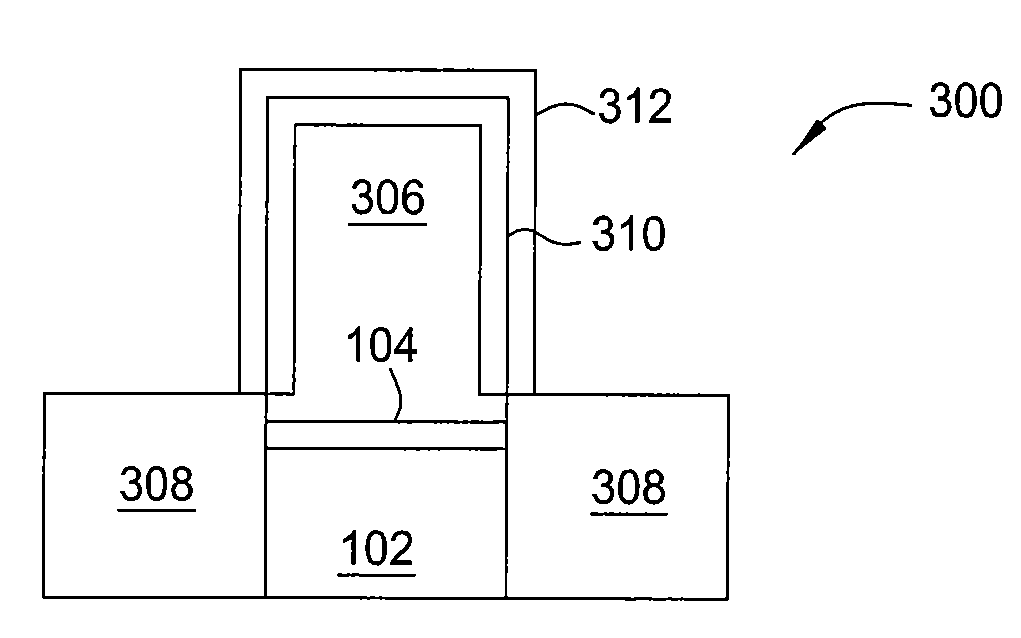
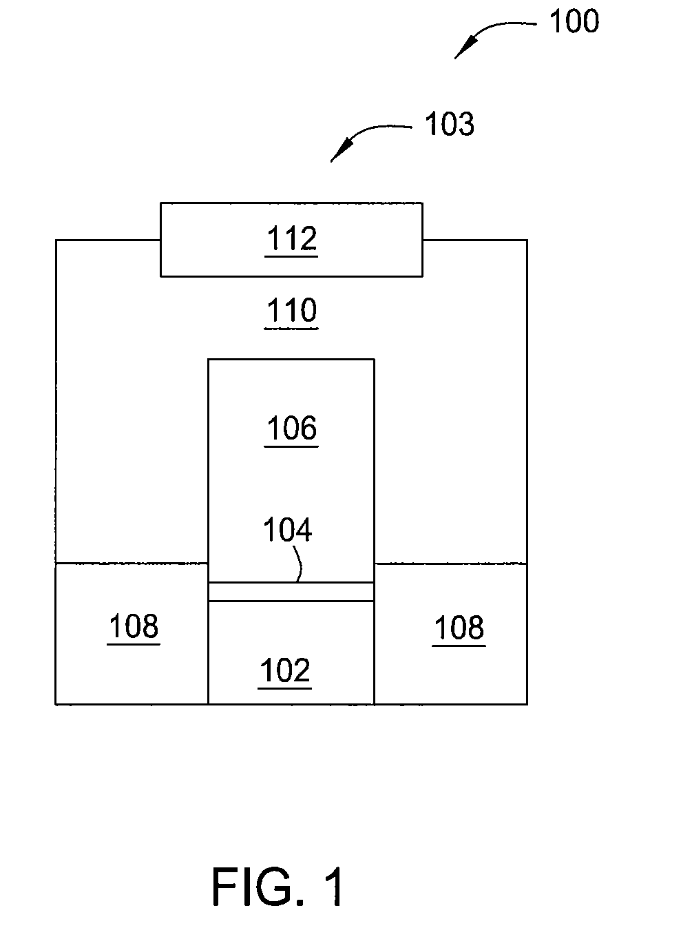
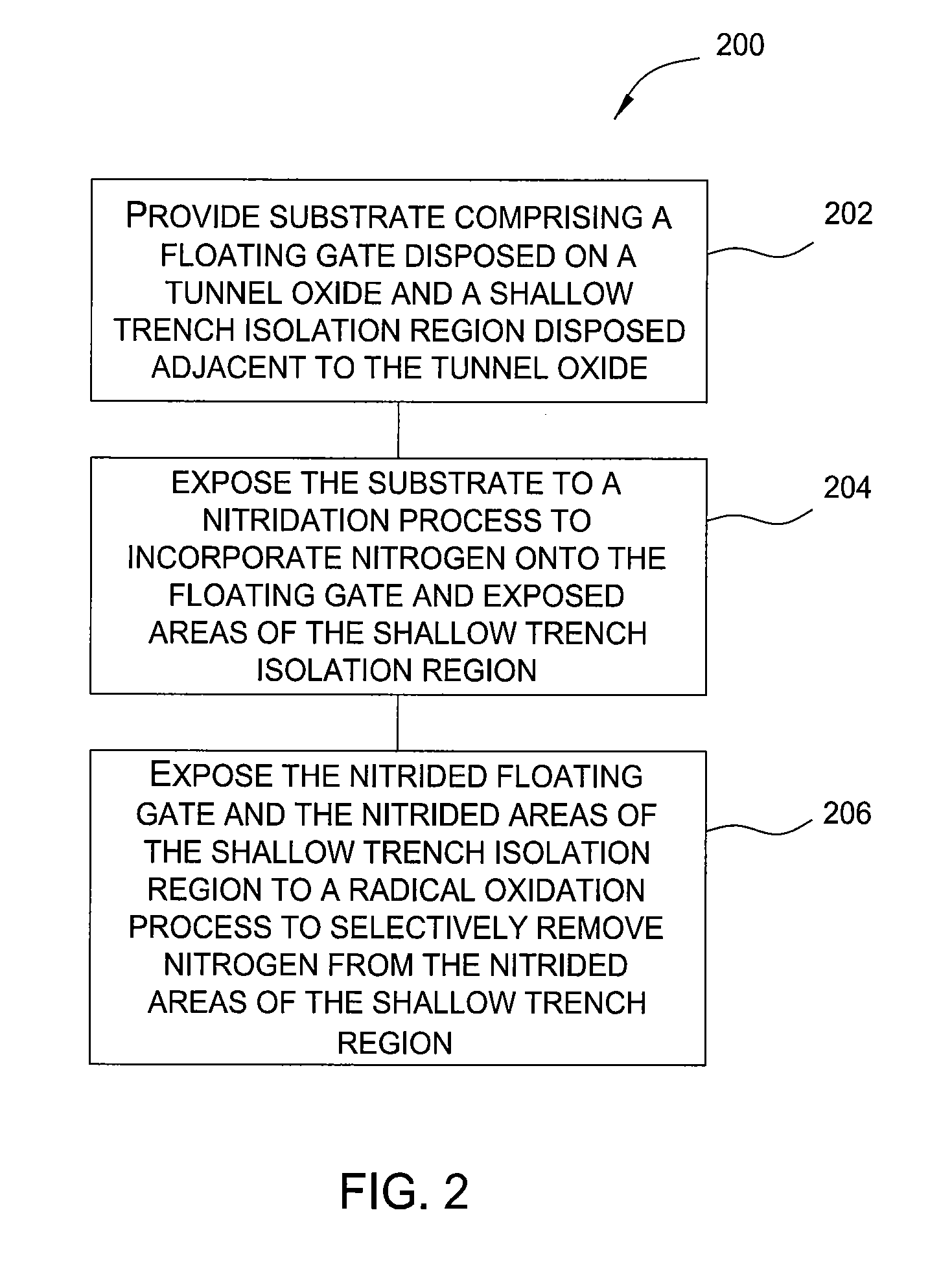
[0027]Embodiments described herein generally relate to the field of semiconductor manufacturing processes and devices. More particularly, the embodiments described herein are related to the selective removal of nitrogen from the nitrided areas of a substrate. Embodiments described herein further provide methods for “selectively nitriding” a substrate by the selective removal of nitrogen from a material layer after a nitridation process without affecting the nitrogen deposited in an oxide containing layer by exposing the material layer to a radical oxidation process. The methods described herein may be used in the production of semiconductor devices, for example, NAND or NOR flash memory, or other suitable devices where selective nitridation of the device is desirable.

[0028]The FG polysilicon is typically doped with phosphorus or boron to provide a conducting film. During subsequent high temperature processing in forming the IPD stack, the dopant can diffuse out from the FG polysilic...


PUM


Abstract

Embodiments described herein generally relate to flash memory devices and methods for manufacturing flash memory devices. In one embodiment, a method for selective removal of nitrogen from the nitrided areas of a substrate is provided. The method comprises positioning a substrate comprising a material layer disposed adjacent to an oxide containing layer in a processing chamber, exposing the substrate to a nitridation process to incorporate nitrogen onto the material layer and the exposed areas of the oxide containing layer, and exposing the nitrided material layer and the nitrided areas of the oxide containing layer to a gas mixture comprising a quantity of a hydrogen containing gas and a quantity of an oxygen containing gas to selectively remove nitrogen from the nitrided areas of the oxide containing layer relative to the nitrided material layer using a radical oxidation process.

Description

CROSS-REFERENCE TO RELATED APPLICATIONS[0001]This application claims benefit of U.S. provisional patent application Ser. No. 61 / 187,208 (Attorney Docket No. 14477L), filed Jun. 15, 2009, which is herein incorporated by reference in its entirety.BACKGROUND[0002]1. Field[0003]Embodiments described herein generally relate to the field of semiconductor manufacturing processes and devices. More particularly, the embodiments described herein are related to the selective removal of nitrogen from the nitrided areas of a substrate.[0004]2. Description of the Related Art[0005]As semiconductor devices continue to scale down according to Moore's Law, processing challenges develop. One such challenge arises in floating gate (FG) NAND flash memory chips, which feature transistors that incorporate two gate elements, a control gate (CG) and a floating gate (FG), to enable each transistor to assume more than one bit value. FG NAND memory forms the basis of most USB flash memory devices and memory ca...

Claims


Application Information

Patent Timeline
IPC IPC(8): H01L21/28H01L21/31
CPCH01L21/28273H01L29/7881H01L29/66825H01L29/40114Y10S438/911
Inventor SWENBERG, JOHANESCHU, DAVIDGUARINI, THERESA KRAMERCHO, YONAHGANGULY, UDAYANDATE, LUCIEN
Owner APPLIED MATERIALS INC
Why Eureka
Try Eureka