
Inhibition of copper dissolution for lead-free soldering

a technology of lead-free soldering and copper dissolution, which is applied in the direction of manufacturing tools, soldering apparatus, transportation and packaging, etc., can solve the problems of compromising the integrity and reliability of the interconnect structure, causing a significant portion of the copper plating layer to dissolve in the solder during the solder reflow process, and further solder-induced copper consumption

Inactive Publication Date: 2010-12-23
AGERE SYST INC
View PDF8 Cites 8 Cited by
  • Summary
  • Abstract
  • Description
  • Claims
  • Application Information

AI Technical Summary

Benefits of technology

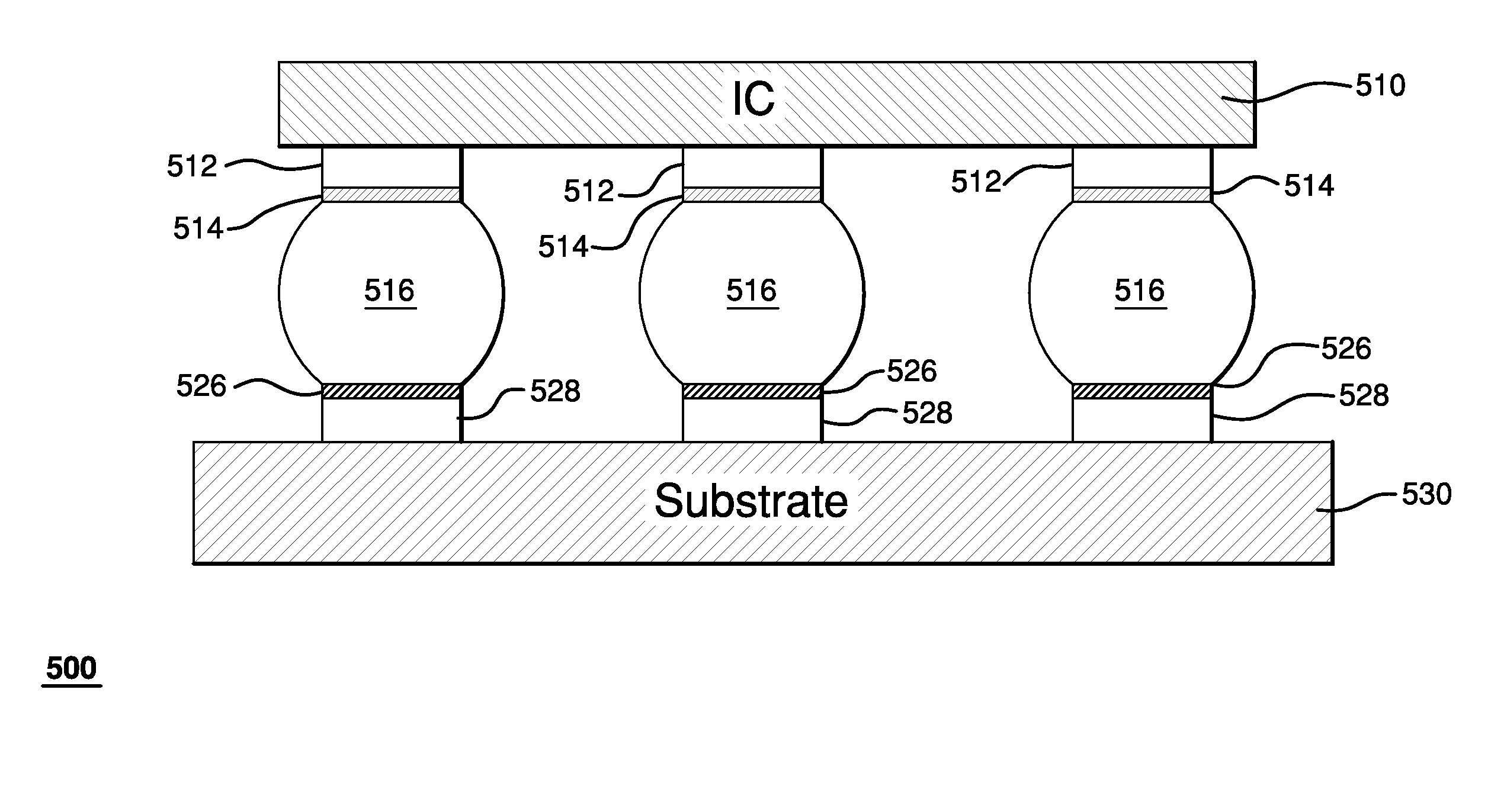
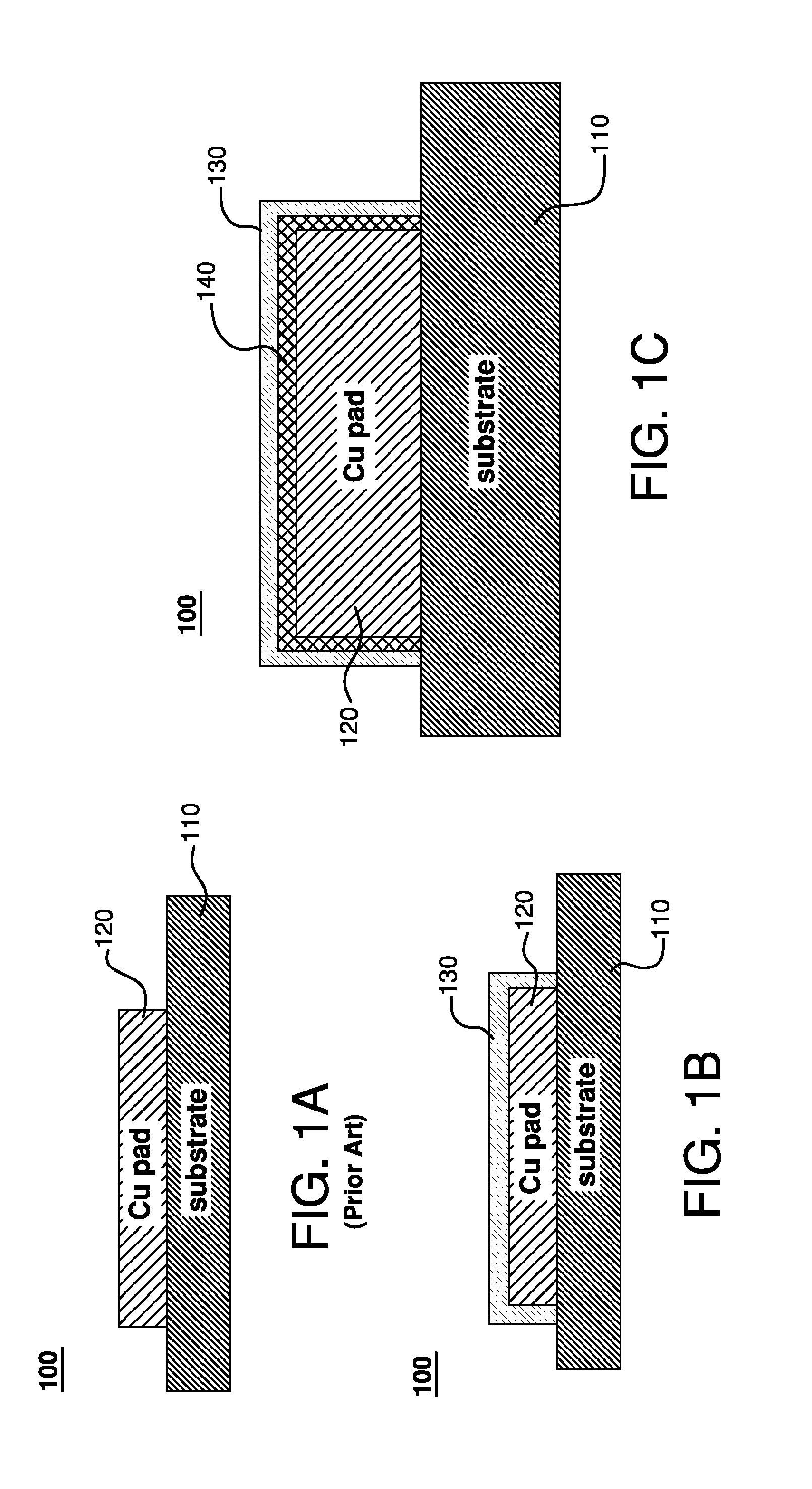
[0007]Problems in the prior art are addressed by various embodiments of a device fabrication method, according to which a tin-copper-alloy layer is formed adjacent to a copper-plated pad or pin that is used to electrically connect the device to external wiring. Advantageously, the tin-copper-alloy

Problems solved by technology

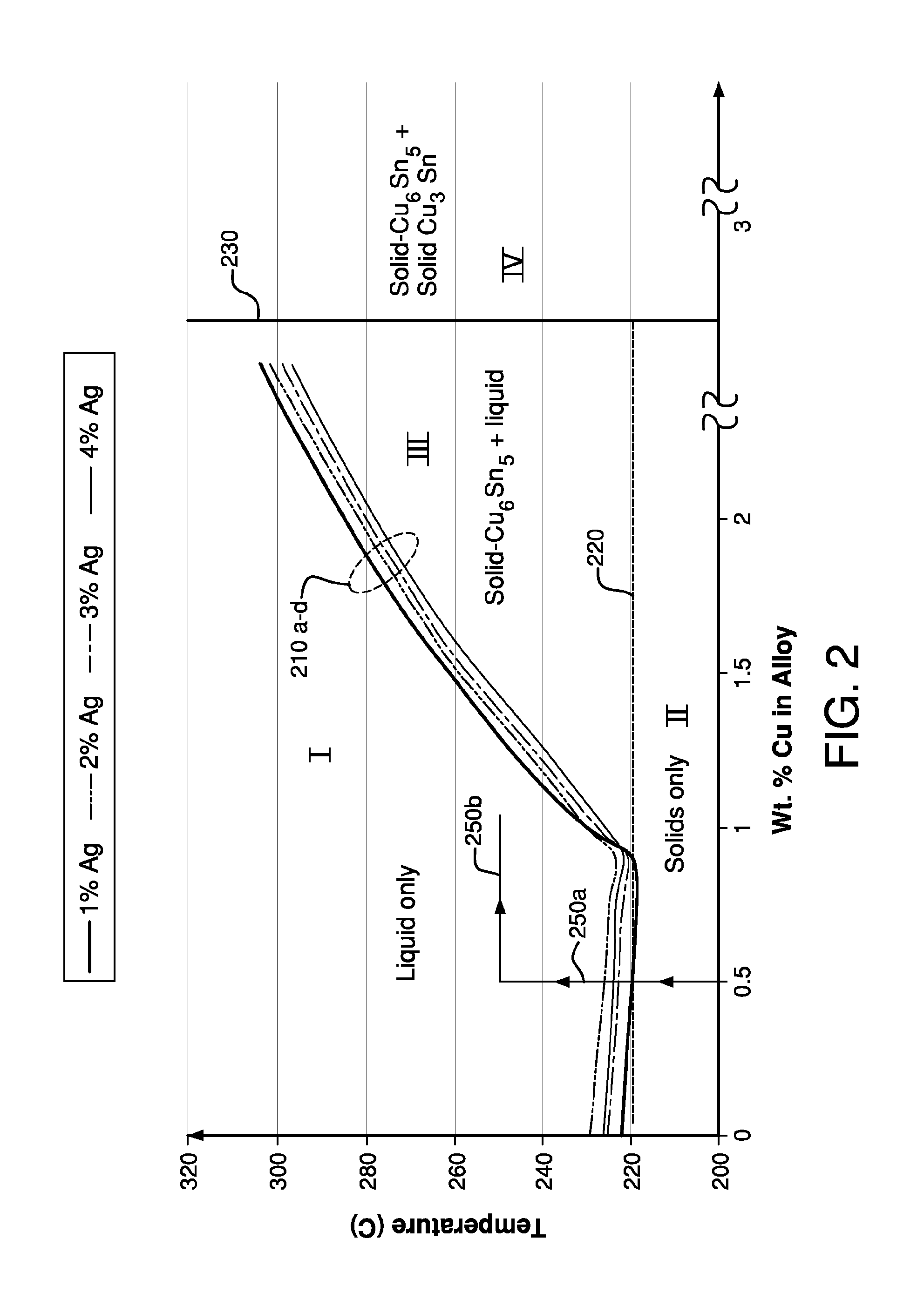
One problem with tin-silver-copper alloys is that, when they are used to solder parts (e.g., contact pads) having copper plating, a tin-silver-copper solder can cause a significant portion of a copper-plating layer to dissolve in the solder during the solder reflow process.
Subsequent exposure to field conditions leads to further solder-induced copper consumption via solid-state formation of copper-tin intermetallics.
All these processes can disadvantageously compromise integrity and reliability of interconnect structures to a point where the device can no longer meet customer requirements.

Method used


Image

  • Inhibition of copper dissolution for lead-free soldering
  • Inhibition of copper dissolution for lead-free soldering
  • Inhibition of copper dissolution for lead-free soldering

Examples


Embodiment Construction

[0017]FIGS. 1A-C schematically show a device fabrication method according to one embodiment of the invention. More specifically, each of FIGS. 1A-C shows a cross-sectional view of a device 100 having a copper pad (or layer) 120 that is used to mechanically and / or electrically attach the device to external wiring (not shown in FIG. 1), e.g., an electrical interconnect structure of a circuit board or chip package. In various embodiments, device 100 can be part of a flip-chip package, a ball-grid-array (BGA) package, a circuit board, etc. One skilled in the art will appreciate that various electronic packages, parts, and components, such as copper-lead frame devices, copper heat sinks, and other devices that have copper, solder, and / or tin as part or all of an interconnect structure connecting one part of an electrical circuit to another part of the circuit, can also be fabricated using embodiments of the method of FIG. 1. Further examples of systems suitable for the application of the...


PUM

PropertyMeasurementUnit
Temperatureaaaaaaaaaa

Abstract

A device fabrication method, according to which a tin-copper-alloy layer is formed adjacent to a copper-plated pad or pin that is used to electrically connect the device to external wiring. Advantageously, the tin-copper-alloy layer inhibits copper dissolution during a solder reflow process because that layer is substantially insoluble in liquid Sn—Ag—Cu (tin-silver-copper) solder alloys under typical solder reflow conditions and therefore shields the copper plating from direct physical contact with the liquefied solder.

Description

BACKGROUND OF THE INVENTION[0001]1. Field of the Invention[0002]The present invention relates generally to fabrication of electronic devices and, more specifically, to methods of forming interconnect structures for microelectronic packages and circuit boards.[0003]2. Description of the Related Art[0004]Restriction of Hazardous Substances (RoHS) is a European legislation that is aimed at eliminating or severely curtailing the use of cadmium, hexavalent chromium, and lead in virtually all consumer products, from automobiles to microelectronic devices. Many other countries, including the United States, are at various stages of introducing comparable pieces of legislation having similar bans on these substances. RoHS effectively requires electronics manufacturers to replace lead-based terminations on electronic devices and packages with lead-free substitutes.[0005]Tin-silver-copper alloys, also referred to as SAC (short for Sn—Ag—Cu) alloys, are the primary choice for lead-free terminat...

Claims


Application Information

Patent Timeline
IPC IPC(8): H05K1/09B05D3/02C22F1/08B23K31/02B32B15/01
CPCH05K3/244H05K3/3463H05K2203/1105H01L2224/16Y10T428/12715H01L2924/01327H01L2924/3025H01L2924/00H01L2224/0508H01L2224/05568H01L2224/05023H01L2224/05001H01L2224/05124H01L2224/05166H01L2224/056H01L24/05H01L24/03H01L2224/0401H01L2224/16503H01L2924/00014
Inventor AMIN, AHMEDBACHMAN, MARK ADAMBAIOCCHI, FRANK A.DELUCCA, JOHN A.OSENBACH, JOHN W.XIONG, ZHENGPENG
Owner AGERE SYST INC
Learn More