Separation method of nitride semiconductor layer, semiconductor device, manufacturing method thereof, semiconductor wafer, and manufacturing method thereof

a technology of nitride semiconductor and semiconductor layer, which is applied in the direction of polycrystalline material growth, chemically reactive gas growth, crystal growth process, etc., can solve the problem of crystal defects, lattice mismatch of approximately 10% between the nitride semiconductor layer and the sapphire substrate, and the separation surface of the semiconductor epitaxial layer from the sapphire substrate is not sufficiently flat, etc. problem, to achieve the effect of facilitating the separation of the nitrid

Inactive Publication Date: 2010-12-23
OKI DATA CORP
View PDF5 Cites 51 Cited by
  • Summary
  • Abstract
  • Description
  • Claims
  • Application Information

AI Technical Summary

Benefits of technology

[0015]The present invention is intended to provide a separation method of a nitride semiconductor layer, a semiconductor devi

Problems solved by technology

In this method, however, a separation surface of the semiconductor epitaxial layers separated from the sapphire substrate does not have a sufficient flatness (i.e., on the order of nanometers).
However, in the method disclosed in Patent Document No. 2, there is a lattice mismatch of approximately 10% between the nitride sem

Method used


Image

  • Separation method of nitride semiconductor layer, semiconductor device, manufacturing method thereof, semiconductor wafer, and manufacturing method thereof
  • Separation method of nitride semiconductor layer, semiconductor device, manufacturing method thereof, semiconductor wafer, and manufacturing method thereof
  • Separation method of nitride semiconductor layer, semiconductor device, manufacturing method thereof, semiconductor wafer, and manufacturing method thereof

Examples


first embodiment

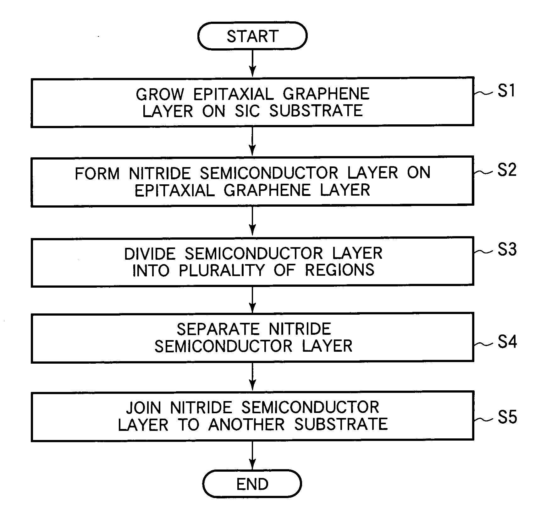
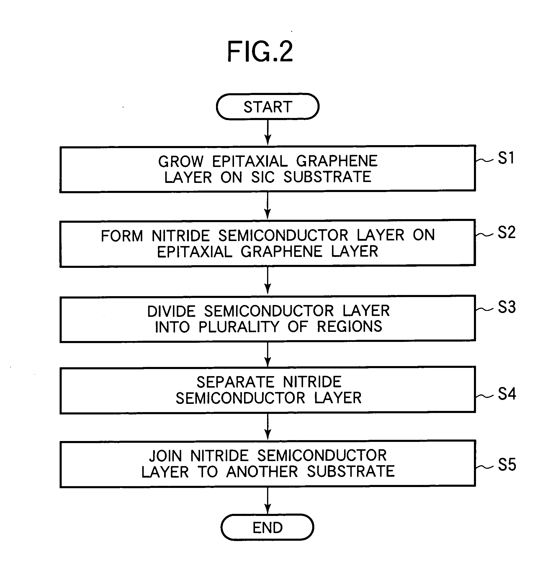
[0054]FIGS. 1A through 13B are views for illustrating a separation method of a semiconductor layer (i.e., a semiconductor thin film) and a manufacturing method of a nitride semiconductor device according to the first embodiment of the present invention.

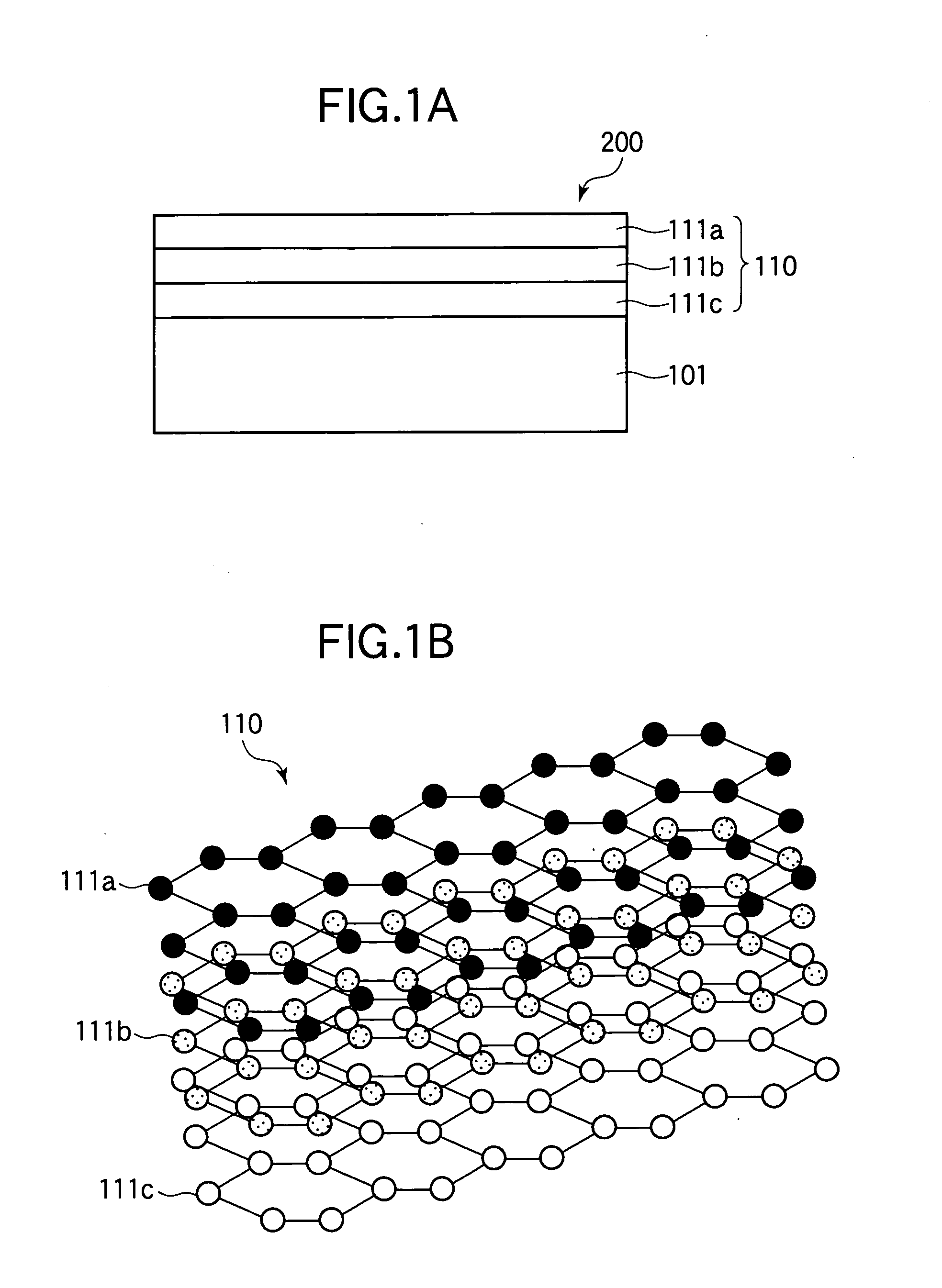
[0055]FIG. 1A shows a graphene-layer-grown substrate 200 (i.e., a substrate with an epitaxial graphene layer) according to the first embodiment of the present invention. The graphene-layer-grown substrate 200 includes a SiC substrate 101 as a first substrate (i.e., a semiconductor substrate) and an epitaxial graphene layer 110 formed on the substrate 101. The epitaxial graphene layer 110 is in the form of a single layer, or two or more layers. In this example, the epitaxial graphene layer 110 includes three graphene layers 111a, 111b and 111c.

[0056]FIG. 1B schematically shows a structure of the epitaxial graphene layer 110. The epitaxial graphene layer 110 includes three graphene layers 111a, 111b and 111c which are layered. The grap...

second embodiment

[0097]In the second embodiment of the present invention, a description will be made of a process in which the nitride semiconductor layer 114 is divided into a plurality of regions having predetermined shapes. The drawings of the first embodiment are herein referred to as necessary.

[0098]As was described in the first embodiment, the epitaxial graphene layer 110 is grown on the SiC substrate 101 (i.e., the first substrate), and the nitride semiconductor layer 114 is grown on the epitaxial graphene layer 110. The nitride semiconductor layer 114 is configured as, for example, the nitride semiconductor layer 114A, 114B, 114C, 114D, 114E, 114F or 114G shown in FIGS. 4A through 6F.

[0099]The nitride semiconductor layer 114 is fabricated into predetermined element shapes so that a plurality of elements are formed on the nitride semiconductor layer 114.

[0100]In FIG. 15, the nitride semiconductor layer 114 is divided into a plurality of element formation regions 214 and a non-element formatio...

third embodiment

[0107]The third embodiment of the present invention is different from the first and second embodiment in the following aspects. The nitride semiconductor layer 114 is grown on the epitaxial graphene layer 110 having been grown on the SiC substrate 101 (i.e., the first substrate), so as to form a nitride-semiconductor-layer / graphene-layer grown substrate 400. Then, a surface of the nitride-semiconductor-layer / graphene-layer grown substrate 400 (i.e., a surface of the nitride semiconductor layer 114 opposite to the graphene layer 111a side) is joined to the surface of another substrate, i.e., the second substrate 130 (or the joining layer 432 formed on the surface of the second substrate 130). Thereafter, the SiC substrate 101 is separated from the nitride semiconductor layer 104. Hereinafter, the third embodiment will be described with reference to FIGS. 18A, 18B, 19A and 19B.

[0108]FIG. 18A shows a process in which the nitride-semiconductor-layer / graphene-layer grown substrate 400 (i...


PUM


Abstract

In a separation method of a nitride semiconductor layer, a graphene layer in the form of a single layer or two or more layers is formed on a surface of a first substrate. A nitride semiconductor layer is formed on the graphene layer so that the nitride semiconductor layer is bonded to the graphene layer with a bonding force due to regularity of potential at atomic level at an interface therebetween without utilizing covalent bonding. The nitride semiconductor layer is separated from the first substrate with a force which is greater than the bonding force between the nitride semiconductor layer and the graphene layer, or greater than a bonding force between respective layers of the graphene layer.

Description

BACKGROUND OF THE INVENTION[0001]The present invention relates to a separation method of nitride semiconductor layer, a semiconductor device and a manufacturing method thereof.[0002]The present invention also relates to a semiconductor wafer, and a manufacturing method thereof.[0003]As an example of a conventional manufacturing method of a semiconductor device, Patent Document No. 1 discloses a manufacturing method of an LED (Light Emitting Diode), in which a buffer layer, an n-type nitride semiconductor layer, an active layer, a p-type nitride semiconductor layer, an n-type contact layer are grown on a sapphire substrate in this order so as to form a semiconductor wafer. Further, these layers are etched so as to partially remove the n-type contract layer, the p-type nitride semiconductor layer and the active layer, and to expose the n-type nitride semiconductor layer. Then, an Al (aluminum) electrode is formed on the exposed surface of the n-type nitride semiconductor layer and on ...

Claims


Application Information

Patent Timeline
IPC IPC(8): H01L29/12H01L21/30H01L33/02H01L21/71H01L29/20
CPCH01L21/02378H01L21/02444H01L21/0254H01L21/02612H01L21/0262H01L33/0079H01L21/02664H01L29/16H01L29/1606H01L29/2003H01L33/007H01L21/02631H01L33/0093
Inventor OGIHARA, MITSUHIKOSAGIMORI, TOMOHIKOSAKUTA, MASAAKIHASHIMOTO, AKIHIRO
Owner OKI DATA CORP
Why Eureka
Try Eureka