Pellicle frame and lithographic pellicle

a lithographic and pellicle technology, applied in the field of lithographic pellicle and lithographic pellicle, can solve the problems of deformation of the repeating pattern, impairing the quality, appearance, and difficulty in always keeping the exposure master plate clean, and achieve the effect of suppressing the deformation of the exposure master pla

Active Publication Date: 2010-12-30
SHIN ETSU CHEM IND CO LTD +1
View PDF8 Cites 5 Cited by
  • Summary
  • Abstract
  • Description
  • Claims
  • Application Information

AI Technical Summary

Benefits of technology

[0014]It is a first object of the present invention to provide a pellicle frame that can suppress deformation of an exp

Problems solved by technology

In the production of a semiconductor such as an LSI or a ULSI or the production of a liquid crystal display panel, a pattern is formed by irradiating a semiconductor wafer or a liquid crystal master plate with light; if debris is attached to an exposure master plate, since the debris absorbs the light or refracts the light, there are problems that the replicated pattern is deformed, the edges become rough, or the background is stained black, thus impairing the dimensions, quality, appearance, etc.
These operations are usually carried out in a clean room, but even within a cl

Method used


Image

  • Pellicle frame and lithographic pellicle
  • Pellicle frame and lithographic pellicle
  • Pellicle frame and lithographic pellicle

Examples


example 1

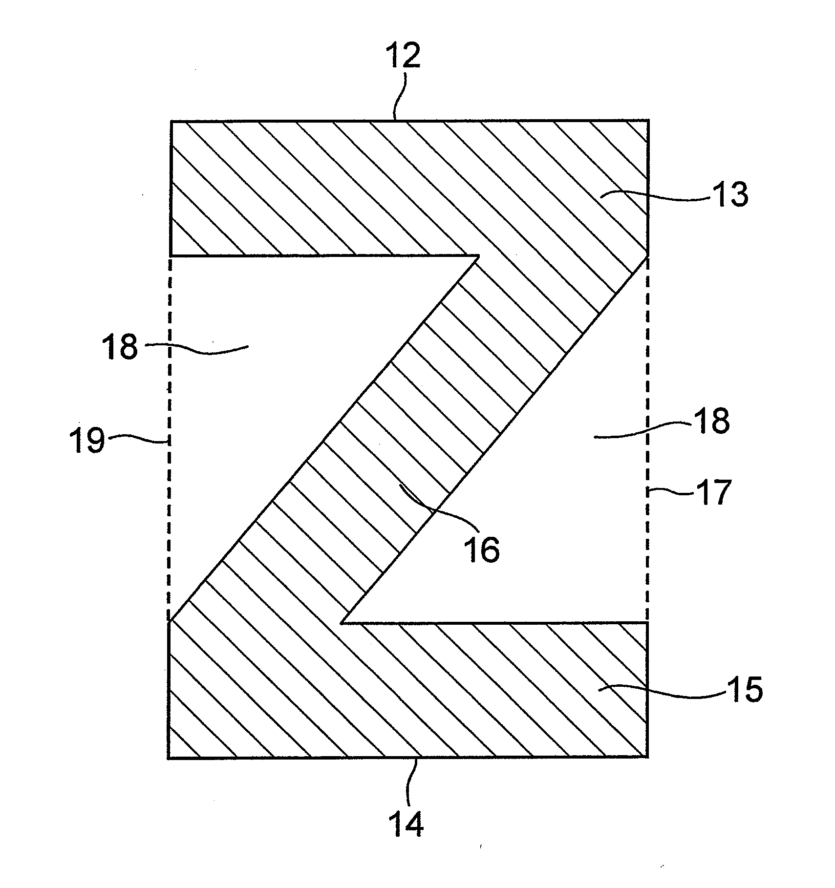
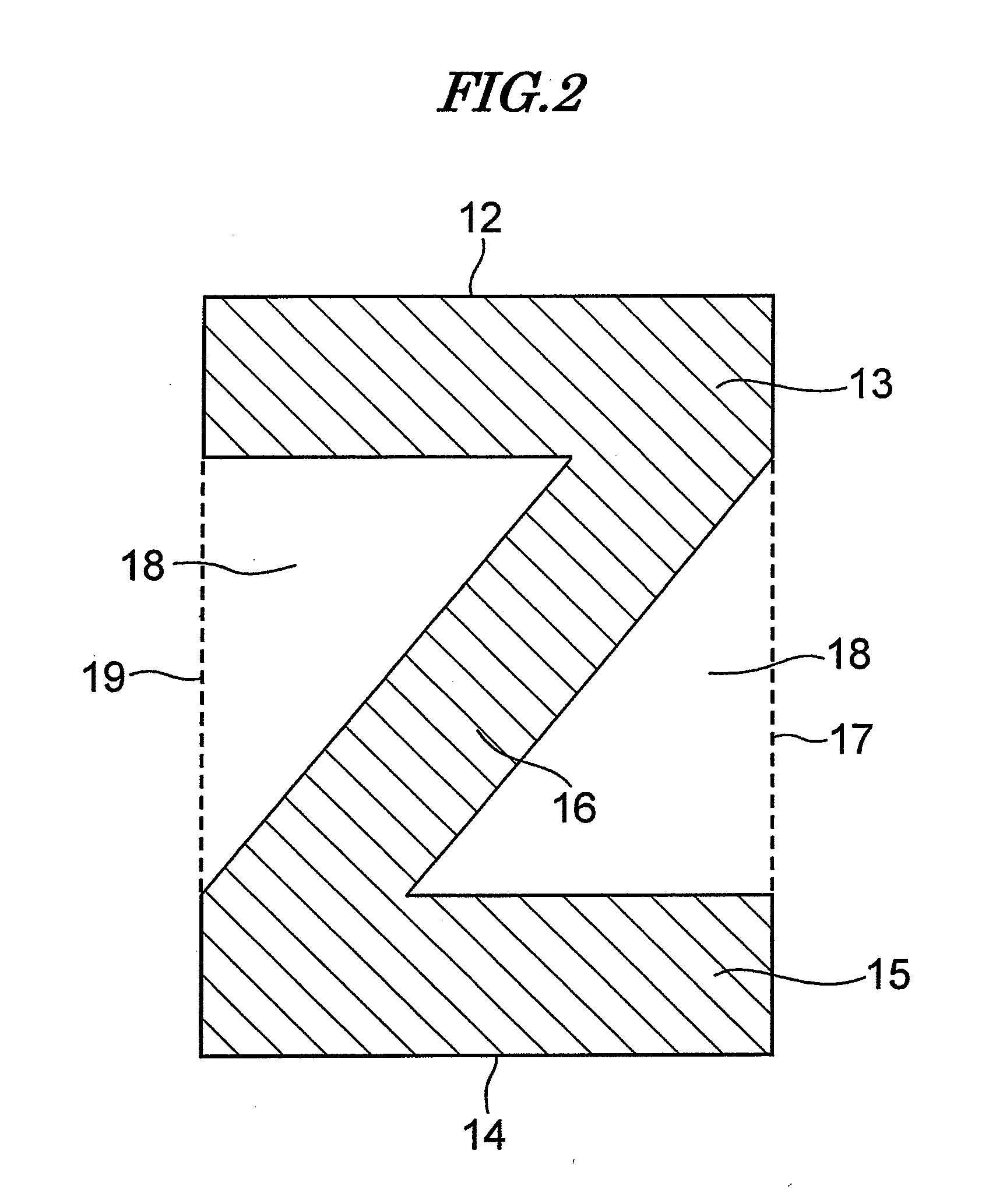
[0093]A pellicle frame with outer dimensions of 149 mm×122 mm×3.5 mm and a width of the upper edge and lower edge of 2 mm was prepared from an aluminum alloy (the cross-sectional shape being shown in FIG. 4 (a), and the cross-sectional area being 3.25 mm2). The cross-sectional shape was a Z shape obtained by removing right-angled triangles having a height of 2.5 mm and a width of an upper edge (lower edge) of 1.5 mm from opposite side faces of a rectangle having a height of 3.5 mm and a width of 2.0 mm in a staggered manner on opposite sides of a central part. The thickness of the upper end part and lower end part was 0.5 mm, and the width in the horizontal direction of the middle part was also 0.5 mm. Four corners of the pellicle frame were subjected to C-chamfering.

[0094]When the flatness of this frame was measured from the side that was to be coated with a mask pressure-sensitive adhesive, it was found to be 20 μm. One end face of the frame was coated with the mask pressure-sensi...

example 2

[0099]A pellicle frame having the same cross-sectional shape as Example 1 with outer dimensions of 149 mm×122 mm×3.5 mm and a width of the upper edge and lower edge of 2 mm was prepared from a magnesium alloy (the cross-sectional shape being shown in FIG. 4 (a), and the cross-sectional area being 3.25 mm2). When the flatness of this frame was measured from the side that was to be coated with a mask pressure-sensitive adhesive, it was found to be 20 μm. One end face of the frame was coated with the mask pressure-sensitive adhesive, and the other end face was coated with a film adhesive. Subsequently, the pellicle film previously peeled off was affixed to the film adhesive side of the magnesium alloy frame and the film on the outer periphery of the frame was cut, thus completing a pellicle.

[0100]The pellicle thus completed was affixed to a 142 mm square mask with a flatness of 0.25 μm using a load of 20 kg. Subsequently, when the flatness of the pellicle-equipped mask was measured aga...

example 3

[0101]A pellicle frame having the same cross-sectional shape as Example 1 with outer dimensions of 149 mm×122 mm×3.5 mm and a width of the upper edge and lower edge of 2 mm was prepared from a polycarbonate resin (the cross-sectional shape being shown in FIG. 4 (a), and the cross-sectional area being 3.25 mm2). When the flatness of this frame was measured from the side that was to be coated with a mask pressure-sensitive adhesive, it was found to be 20 μm. One end face of the frame was coated with the mask pressure-sensitive adhesive, and the other end face was coated with a film adhesive. Subsequently, the pellicle film previously peeled off was affixed to the film adhesive side of the polycarbonate resin frame and the film on the outer periphery of the frame was cut, thus completing a pellicle.

[0102]The pellicle thus completed was affixed to a 142 mm square mask with a flatness of 0.25 μm using a load of 20 kg. Subsequently, when the flatness of the pellicle-equipped mask was meas...


PUM


Abstract

A pellicle frame is provided that includes a pellicle frame bar having a cross-section with a shape that has at least one triangular recess in at least one side edge of a quadrilateral having an upper edge and a lower edge parallel to each other and a cross-sectional area of no greater than 20 mm2. There is also provided a lithographic pellicle that includes a pellicle film stretched over one end face of the pellicle frame via a pellicle film adhesive, and that includes an exposure master plate adhesive on the other end face.

Description

TECHNICAL FIELD[0001]The present invention relates to a pellicle frame and a lithographic pellicle used as a debris shield for a lithography mask when producing a liquid crystal display panel or a semiconductor device such as an LSI or a ULSI.BACKGROUND ART[0002]In the production of a semiconductor such as an LSI or a ULSI or the production of a liquid crystal display panel, a pattern is formed by irradiating a semiconductor wafer or a liquid crystal master plate with light; if debris is attached to an exposure master plate, since the debris absorbs the light or refracts the light, there are problems that the replicated pattern is deformed, the edges become rough, or the background is stained black, thus impairing the dimensions, quality, appearance, etc. The ‘exposure master plate’ referred to in the present invention is a general term for lithography masks (also called simply ‘masks’) and reticles. The explanation below is given for a mask as an example.[0003]These operations are ...

Claims


Application Information

Patent Timeline
IPC IPC(8): G03B27/62B65D85/86G03F1/64H01L21/027
CPCG03F1/64
Inventor SHIRASAKI, TORUCHAKRAVORTY, KISHOREMUSHELL, DAVIDNG, GRACE
Owner SHIN ETSU CHEM IND CO LTD
Why Eureka
Try Eureka