Phase change memory having one or more non-constant doping profiles

a phase change memory and non-constant technology, applied in the field of memory devices, can solve problems such as reducing the overall resistance of the cell

Active Publication Date: 2010-12-30
IBM CORP +1
View PDF99 Cites 64 Cited by
  • Summary
  • Abstract
  • Description
  • Claims
  • Application Information

AI Technical Summary

Benefits of technology

[0017]A phase change memory device is described herein with a memory element including a basis phase change material, such as a chalcogenide like GST, and one or more additives, where the additive or additives have a non-constant concentration profile along an inter-electrode current path through a memory element. The device includes a first electrode, a phase change memory element in contact with the first electrode, and a second electrode in contact with the memory element. The memory element has a body of phase change material that can be characterized as having zones which are subject to different thermal and

Problems solved by technology

Also, the absence of silicon doping in the seco

Method used


Image

  • Phase change memory having one or more non-constant doping profiles
  • Phase change memory having one or more non-constant doping profiles
  • Phase change memory having one or more non-constant doping profiles

Examples


first embodiment

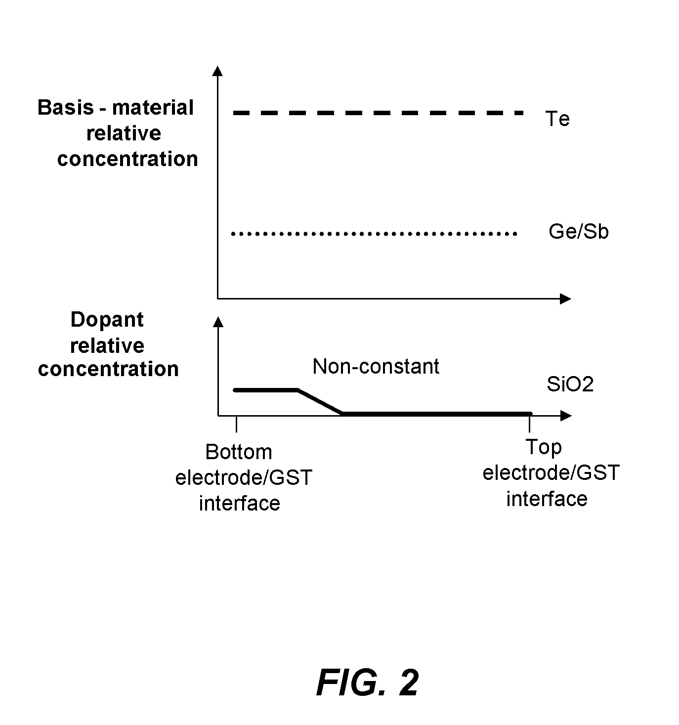
[0038]FIG. 2 illustrates the non-constant additive concentration profile using silicon oxide as an additive. As can be seen in FIG. 2, the concentration of SiO2 is higher at the interface between the bottom electrode 120 and the memory element 116, than at the interface between the top electrode 140 and the memory element 116. In the illustrated example of FIG. 2 additives of the phase change material at the interface between the bottom electrode 120 and the memory element 116 have an Si concentration of about 5 at %+ / −2% at, and an O concentration of about 10 at %+ / −4 at %. The concentration of SiO2 then transitions downward to substantially undoped GST at the interface with the top electrode, resulting in the non-constant additive concentration profile as shown.

[0039]The active region 110 comprises phase change material domains within a dielectric-rich mesh (not shown), caused by separation of the silicon oxide doping from the phase change alloy, as described in detail in U.S. pat...

second embodiment

[0045]FIG. 3 illustrates a non-constant additive concentration profile using a composite doping of silicon oxide and silicon. In the illustrated example of FIG. 3, the silicon oxide additive of the phase change material at the interface between the bottom electrode 120 and the memory element 116 has a Si concentration of about 5 at %+ / −2% at, and an O concentration of about 10 at %+ / −4 at %. The maximum silicon additive in this example is between about 1 to 5 at % in addition to the silicon that is counted part of the silicon dioxide. Thus, a consolidated concentration profile for the elements silicon and oxygen, along with the GST basis material can include at 10% silicon, 10 at % oxygen and 80 at % for the combination of the elements of GST. It is found that silicon additives improve retention time and endurance, but can retard set time. Putting higher concentrations of silicon within the active region 110 can improve retention in the active region, while for regions far away from...

third embodiment

[0046]FIG. 4 illustrates a non-constant additive concentration profile using a composite doping of silicon oxide and silver. In the illustrated example of FIG. 4 the silicon oxide additive of the phase change material at the interface between the bottom electrode 120 and the memory element 116 has a Si concentration of about 5 at %+ / −2% at, and an O concentration of about 10 at %+ / −4 at %. It is found that adding silver can improve retention but can also make the cells' threshold voltage too high for practical implementation in a chip. The non-constant additive concentration profile of silver may lower the threshold voltage to a practical value while still providing good retention for the cell.


PUM


Abstract

A phase change memory device with a memory element including a basis phase change material, such as a chalcogenide, and one or more additives, where the additive or additives have a non-constant concentration profile along an inter-electrode current path through a memory element. The use of “non-constant” concentration profiles for additives enables doping the different zones with different materials and concentrations, according to the different crystallographic, thermal and electrical conditions, and different phase transition conditions.

Description

CROSS-REFERENCE TO RELATED APPLICATIONS[0001]Benefit of U.S. Provisional Application No. 61 / 220,502, filed 25 Jun. 2009 is hereby claimed.BACKGROUND OF THE INVENTION[0002]1. Field of the Invention[0003]The present invention relates to memory devices based on phase change materials including chalcogenide materials, and methods for manufacturing such devices.[0004]2. Description of Related Art[0005]Phase change based memory materials, like chalcogenide based materials and similar materials, can be caused to change between an amorphous phase and a crystalline phase by application of electrical current at levels suitable for implementation in integrated circuits. The amorphous phase is characterized by higher electrical resistivity than the crystalline phase, which can be readily read to indicate data. These properties have generated interest in using programmable resistive material to form non-volatile memory circuits, which can be read and written with random access.[0006]The change f...

Claims


Application Information

Patent Timeline
IPC IPC(8): G11C11/00H01L45/00
CPCG11C13/0004H01L45/06H01L45/1226H01L45/1641H01L45/144H01L45/1625H01L45/1233
Inventor SHIH, YEN-HAOCHENG, HUAI-YUCHEN, CHIEH-FANGWU, CHAO-ILEE, MING-HSIULUNG, HSIANG-LANBREITWISCH, MATTHEW J.RAOUX, SIMONELAM, CHUNG HON
Owner IBM CORP
Why Eureka
Try Eureka