Method for manufacturing electrochemical element electrode

a manufacturing method and electrochemical element technology, applied in the field of electrochemical elements, can solve the problems of undetected wrinkles or ruptures of current collectors, local decline of cell characteristics, and distortion of negative electrodes including current collectors, and achieves the reduction of active material deposited on current collector dents, simple and highly productive methods, and high reliability of charge/discharge cycle characteristics.

Inactive Publication Date: 2010-12-30
PANASONIC CORP
View PDF8 Cites 13 Cited by
  • Summary
  • Abstract
  • Description
  • Claims
  • Application Information

AI Technical Summary

Benefits of technology

[0029]According to the present invention, a space for alleviating the expansion stress of the active material layer is certainly provided between active material bodies, while the contact area size is increased, and so the adherence can be improved, between the active material bodies and the surface of the bumps of the current collector. In addition, the amount of the active material deposited on the dents of the current collector can be decreased.
[0030]Accordingly, the electrode can be suppressed from being distorted, wrinkled or ruptured due to the repetition of charge / discharge, and also the active material bodies can be suppressed from being delaminated from the current collector due to the repetition of charge / discharge. Thus, an electrode for an electrochemical device having highly reliable charge / discharge cycle characteristic and other characteristics can be provided using an active material largely expandable and contractable.
[0031]Also according to the present invention, an electrode as described above can be produced by a simple and highly productive method.

Problems solved by technology

As a result, the negative electrode including the current collector is distorted because of generation of a large stress.
This may undesirably wrinkle or rupture the current collector or delaminate the active material layer from the current collector.
When the negative electrode is distorted or wrinkled, a gap is made between the negative electrode and the separator to cause a non-uniform charge / discharge reaction, which may undesirably cause a local decline of cell characteristics.
In addition, when the active material layer is delaminated from the current collector, the electron conductivity of the negative electrode may be decreased and as a result a sufficiently high charge / discharge cycle characteristic may possibly not be provided.

Method used


Image

  • Method for manufacturing electrochemical element electrode
  • Method for manufacturing electrochemical element electrode
  • Method for manufacturing electrochemical element electrode

Examples


embodiment 1

[0097]A method for producing an electrode for an electrochemical device (hereinafter, referred to simply as the “electrode”) in Embodiment 1 according to the present invention will be described. The electrode for an electrochemical device in this embodiment is a negative electrode for a lithium secondary cell using a silicon oxide as the active material.

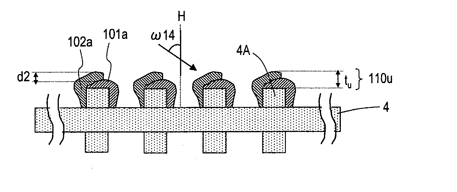
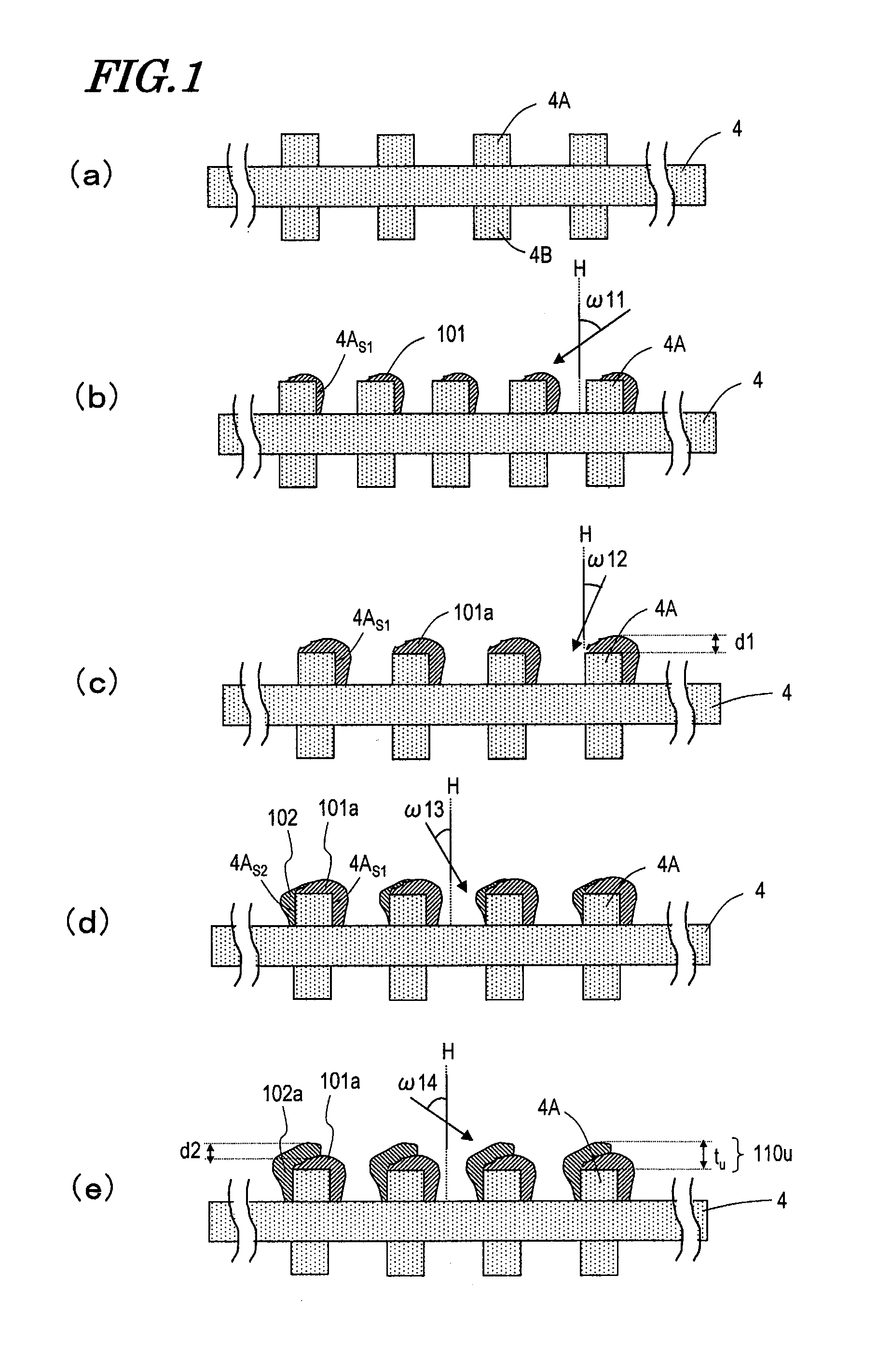
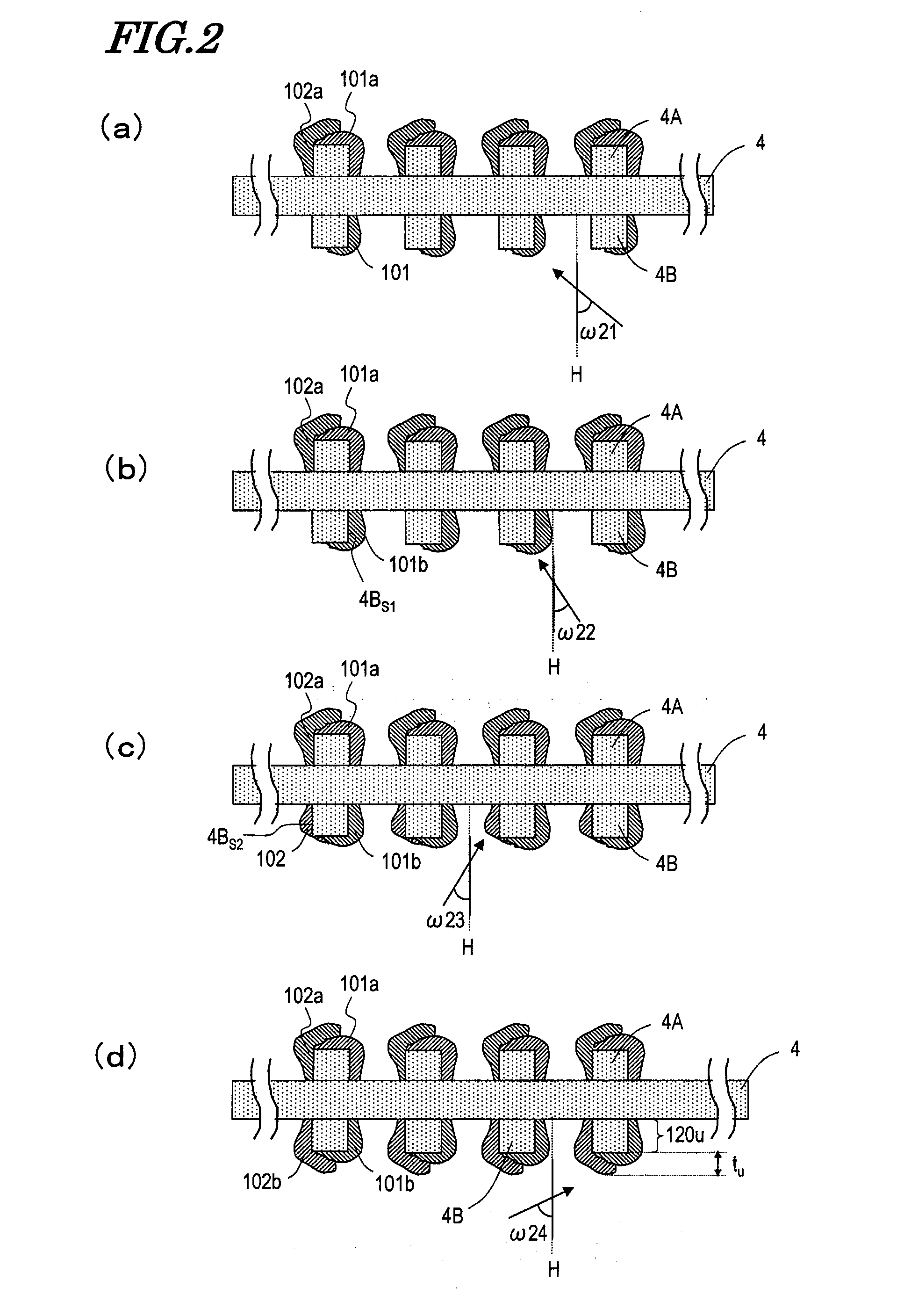
[0098]FIG. 1 though FIG. 5 are schematic cross-sectional views of steps illustrating a method for producing an electrode in this embodiment. FIG. 6(a) is a schematic cross-sectional view showing an example of a vapor deposition apparatus usable for the method in this embodiment, and FIG. 6(b) is a cross-sectional view illustrating an incidence angle ω of a vapor deposition material in the vapor deposition apparatus shown in FIG. 6(a).

[0099]

[0100]First, a vacuum vapor deposition apparatus used in this embodiment will be described. As shown in FIG. 6(a), a vacuum vapor deposition apparatus 50 includes a chamber 1, an evacuation pump 2 ...

example 1

[0182]First, an electrode in Example 1 according to the present invention will be described.

[0183]1. Production of a Current Collector

A copper alloy foil having a thickness of 18 μm (produced by Hitachi Cable Ltd.; Zr amount: 0.02% by weight) was processed with roller press at a cable pressure of 1 ton / cm using a roller having a generally diamond-shaped bottom surface and a plurality of dents. Thus, a current collector having a plurality of bumps on a surface thereof was formed.

[0184]FIGS. 10(a) and 10(b) are respectively a schematic cross-sectional view and a schematic top view of a current collector in Example 1. As shown in the figures, each of bumps 4A was like a rectangular column (average height: 6 μm) having a diamond-shaped top surface (lengths of diagonal: 10 μm×20 μm). A pitch Px of the bumps 4A in an X direction along the shorter diagonal of the diamond shape was 30 μm. Lines of the bumps 4A along the X direction, and another lines of the bumps 4A shifted from the above l...

example 2

[0272]First, an electrode in Reference Example 2 according to the present invention will be described.

[0273]1. Production of a Current Collector

A current collector substantially the same as used in Example 1 was produced by substantially the same method as described above with reference to FIGS. 10(a) and 10(b).

[0274]2. Formation of the Active Material Layer

[0275]An active material layer was formed on both surfaces of the current collector using the vapor deposition apparatus 52 shown in FIGS. 12(a) and 12(b) by substantially the same method as described above with reference to FIGS. 14 and 15. With reference to these figures again, a method for forming the active material layer in this example will be described.

[0276]In this example, in the chamber 1 of the vapor deposition apparatus 52, the rate of the current collector 4 running between the first roller 3 and the second roller 8 was 1 cm / min. As the vaporization source 9, the carbon crucible 10 located below the vapor deposition ...


PUM

PropertyMeasurementUnit
heightaaaaaaaaaa
heightaaaaaaaaaa
incidence angleaaaaaaaaaa

Abstract

Includes the steps of preparing a sheet-like current collector 4 having a plurality of bumps 4A on a surface thereof, the plurality of bumps having a height of 3 μm or greater and 10 μm or less; and forming an active material body having a stacked structure on each of the bumps 4A of the current collector 4. The step of forming the active material body includes a first layer vapor deposition step of causing a vaporized vapor deposition material to be incident on the surface of the current collector 4 in a direction inclined with respect to the normal H to the current collector 4 to form a first layer 101a of the active material body on each bump 4A, the first layer 101a being located closest to the current collector; and a second layer vapor deposition step of causing the vaporized vapor deposition material to be incident on the surface of the current collector 4 in a direction inclined, with respect to the normal H to the current collector 4, opposite to the incidence direction of the vapor deposition material in the first layer vapor deposition step to form a second layer 102a on at least a part of the first layer 101a. In the first layer vapor deposition step, vapor deposition is performed while moving the current collector 4 in a direction in which the incidence angle ω of the vapor deposition material with respect to the normal H to the current collector 4 is decreased.

Description

TECHNICAL FIELD[0001]The present invention relates to an electrode for an electrochemical device including a current collector and an active material carried by the current collector, and a method for producing the same.BACKGROUND ART[0002]Recently, along with the development of portable devices such as personal computers, mobile phones and the like, there is increasing demand for cells as power supplies of these devices. Cells for such uses are desired to have a high energy density and a superb cycle characteristic.[0003]As a response to such a desire, nonaqueous electrolytic lithium secondary cells are now a target of attention, which use any of various types of nonaqueous electrolysis such as, for example, an organic electrolytic solution or a gel polymeric electrolysis obtained by defluidizing an organic electrolytic solution by use of a polymer or a gelating agent as an electrolysis, and use lithium ions as a charge-migrating medium. Usable as a positive electrode material of s...

Claims


Application Information

Patent Timeline
Patent Type & Authority Applications(United States)
IPC IPC(8): H01M4/13H01M4/04B05D5/12H01M10/36
CPCH01M4/0421H01M4/133H01M4/1391Y02T10/7011H01M4/70H01M10/0525Y02E60/122H01M4/1393Y02E60/10
Inventor OGAWA, YUKOHONDA, KAZUYOSHI
Owner PANASONIC CORP
Why Eureka
Try Eureka