Rotational antenna and semiconductor device including the same

a technology of rotating antennas and semiconductor devices, applied in the direction of coatings, coatings, chemical vapor deposition coatings, etc., can solve the problems of increasing manufacturing costs and difficulties, disadvantages of ccp sources in appropriately forming patterns, and affecting the formation of fine patterns on workpieces, so as to minimize the loss of capacitive coupling electromagnetic fields, improve the structure of conventional antenna coils, and uniform plasma density distribution

Active Publication Date: 2011-01-06
ALLIED TECHFINDERS
View PDF12 Cites 380 Cited by
  • Summary
  • Abstract
  • Description
  • Claims
  • Application Information

AI Technical Summary

Benefits of technology

[0021]The present invention improves the conventional antenna coil structure provided in an inductively coupled plasma source and designed to generate a voltage difference, thereby minimizing the loss of a capacitive coupling electromagnetic field which would occur due to a voltage drop. Furthermore, the present invention can accomplish a uniform plasma density distribution by rendering an antenna coil rotatable in an effort to improve the non-uniformity in a plasma density dis

Problems solved by technology

Therefore, the electromagnetic field is apt to adversely affect the formation of a fine pattern on the workpiece.
Furthermore, since the CCP source has plasma generation density smaller than that of the ICP source, the CCP source is disadvantageous in appropriately forming a pattern as a line width grows narrower.
Moreover, as a high level of power is applied to the CCP source, severe damages may be caused to the workpiece and the semicon

Method used


Image

  • Rotational antenna and semiconductor device including the same
  • Rotational antenna and semiconductor device including the same
  • Rotational antenna and semiconductor device including the same

Examples


Embodiment Construction

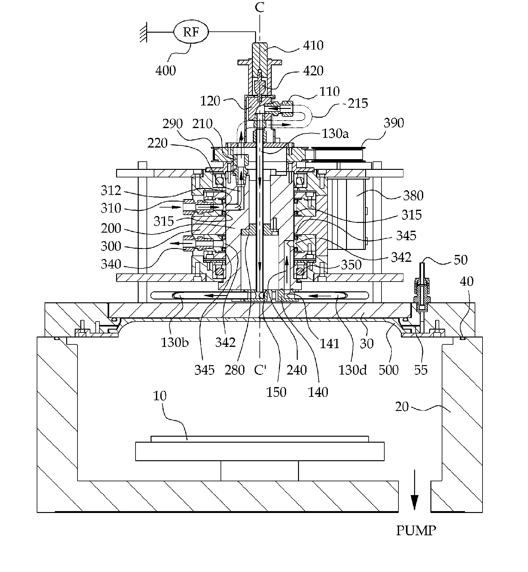
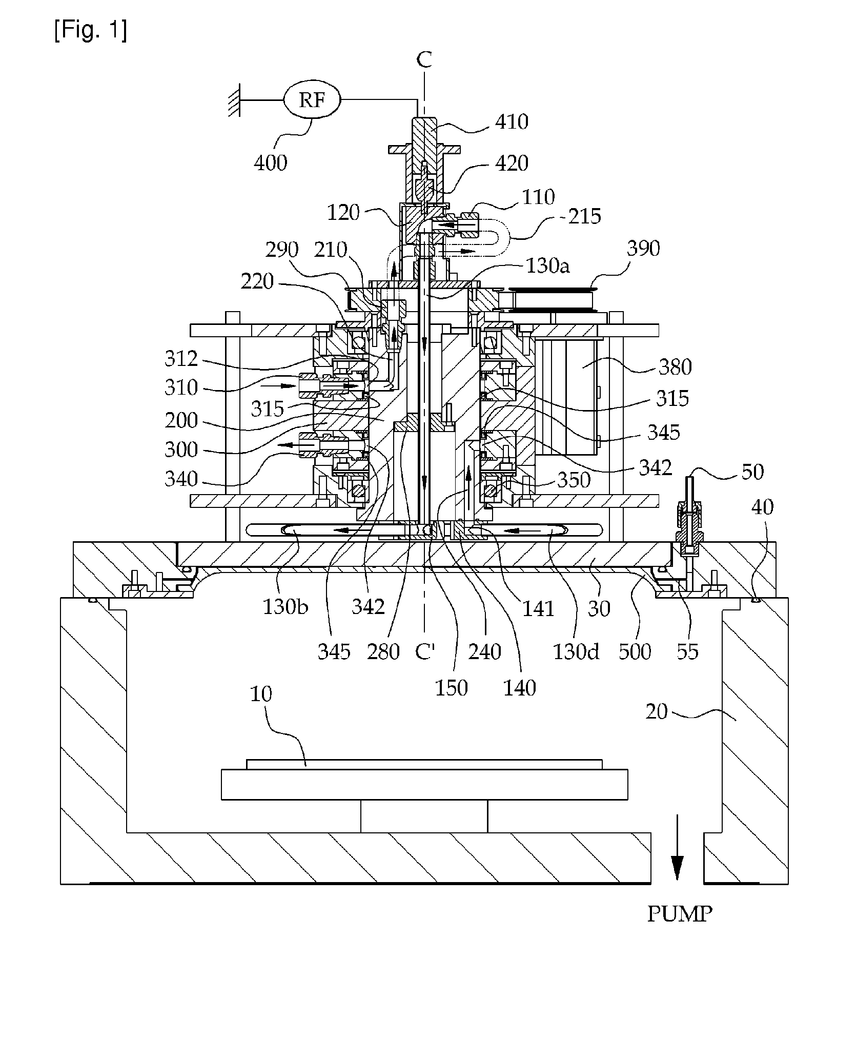
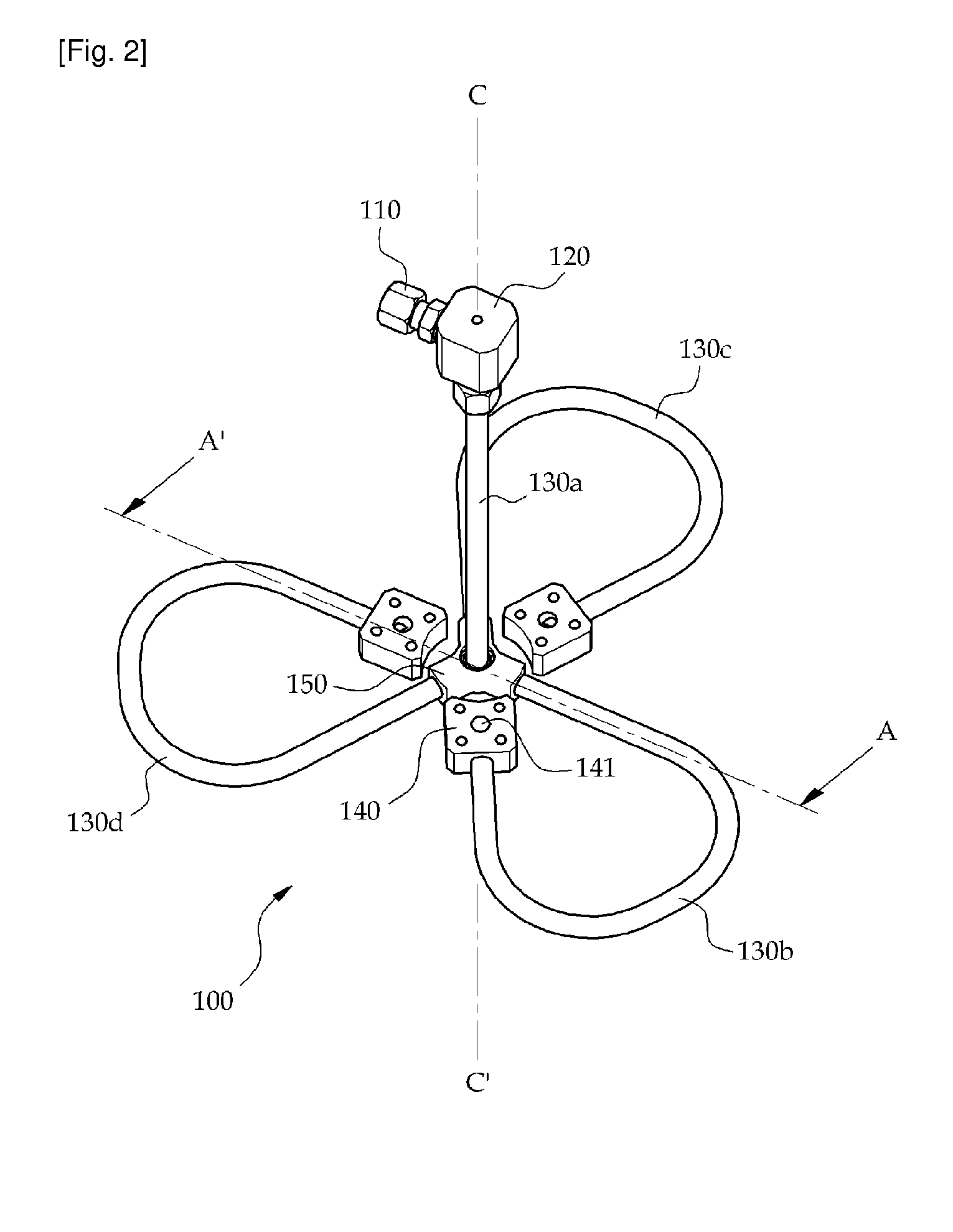
[0031]Hereinafter, embodiments of the present invention will be described in detail with reference to the accompanying drawings. In this regard, it is to be understood that the sizes and the shapes of the components shown in some of the drawings are illustrated in an exaggerated scale for the sake of clarity in explanation. Furthermore, the terms specifically defined herein in consideration of the construction and function of the present invention may have different meanings depending on the intention of a user or operator and the practice in the art. The definitions of these terms shall be construed in terms of the whole description given in this specification.

[0032]The present invention is directed to a plasma source for a large-area workpiece which can be used in processing a circular substrate. Further, the present invention pertains to a plasma source having enhanced adaptability for the size of the circular substrate and, in particular, suitable for use in a semiconductor manu...


PUM

PropertyMeasurementUnit
Poweraaaaaaaaaa
Electric potential / voltageaaaaaaaaaa
Frequencyaaaaaaaaaa

Abstract

A rotational antenna and a semiconductor manufacturing device provided with the same are disclosed. The rotational antenna includes a plurality of coils connected in parallel to a high frequency power source and arranged at a regular interval around an axis in a symmetrical relationship with respect to the axis, wherein an electromagnetic field for generating inductively coupled plasma is uniformly formed when the coils are rotated about the axis.

Description

TECHNICAL FIELD[0001]The present invention relates to a rotational antenna provided as a plasma source in semiconductor manufacturing devices, such as etching devices or deposition devices (including a plasma enhanced chemical vapor deposition device, a high density plasma chemical vapor deposition device and a plasma enhanced atomic layer deposition device), which are used to process a substrate using plasma (hereinafter, the term substrate is used to cover a wafer and an LCD glass substrate). And the present invention relates to a semiconductor manufacturing device having the rotational antenna as a plasma source.BACKGROUND ART[0002]Plasma sources for use in forming fine patterns on the surfaces of substrates have been developed into various shapes in view of the necessity of finely forming the line width of a circuit pattern in the field of semiconductors and in view of the necessity of increasing the size of a glass substrate in the field of LCDs made of glass substrates.[0003]T...

Claims


Application Information

Patent Timeline
IPC IPC(8): H01L21/465H01L21/46
CPCH01J37/321H05H1/46H01J37/32568H01J37/3211H01J37/32522H05H1/4652C23C16/507
Inventor SUH, KEE WON
Owner ALLIED TECHFINDERS
Why Eureka
Try Eureka