Method for treating surface of soi substrate

a technology of soi substrate and surface treatment, which is applied in the direction of basic electric elements, electrical equipment, semiconductor devices, etc., can solve the problems of difficult improvement, difficult to achieve nanometer-scale accuracy with a high yield, and methods with disadvantages, so as to suppress the action of etching and enhance the uniformity of film thickness. , the effect of suppressing the variation of the film thickness of the soi substra

Inactive Publication Date: 2011-01-06
SHIN ETSU CHEM IND CO LTD
View PDF9 Cites 10 Cited by
  • Summary
  • Abstract
  • Description
  • Claims
  • Application Information

AI Technical Summary

Benefits of technology

[0022]As described above, in accordance with the method for treating a surface of a SOI substrate and the method for producing a bonded wafer according to the present invention, the anneal step of applying a heat treatment in argon atmosphere or an inert gas atmosphere containing 4 vol % or less of hydrogen can be carried out to suppress the action of etching more than in the anneal step of applying a heat treatment in an atmosphere of 100% hydrogen.
[0023]Therefore, the surface can be smoothed to a desired surface roughness while suppressing the film thickness variation of the SOI substrate which has uniformity in film thickness enhanced through the treatment by the PACE method or the GCIB method.
[0024]In addition, when the concentration of the hydrogen contained in the inert gas is 4 vol % or less, the etching effect is suppressed. The hydrogen concentration of not more than the lower explosion limit enables relatively safe handling of hydrogen gas.
[0025][FIG. 1] In-plane thickness variation of SOI film before and after PACE treatment, and after annealing (at 1100° C. for 4 hours) in each atmosphere
[0026][FIG. 2] The amount of silicon etched (represented by thickness decrease) by anneal (at 1100° C. for 4 hours) in each atmosphere
[0027][FIG. 3] Surface roughness after annealing (at 1100° C. for 4 hours) in each atmosphere

Problems solved by technology

However, it is practically difficult to achieve the nanometer-scale accuracy with a high yield, and it is difficult to make an improvement as it now stands.
However, these methods have disadvantages at the same time.
The in-plane uniformity in film thickness might deteriorate in the process of the polishing.

Method used


Image

  • Method for treating surface of soi substrate
  • Method for treating surface of soi substrate
  • Method for treating surface of soi substrate

Examples


example 1

[0054]A SOI substrate was produced as follows in accordance with the method for producing a SOI substrate according to the bonding method.

[0055]First, a SOI substrate was prepared by the SiGen method (step a).

[0056]In this step, a silicon wafer with an ion-implanted region formed by implanting hydrogen ions under the implantation conditions: an implantation energy of 35 keV; an implantation dose of 9×10¹⁶ / cm2; and an implantation depth of 0.3 μm was prepared as a donor wafer, whereas a synthetic quartz substrate was prepared as a handle wafer, and the surfaces to be attached were subjected to a high-frequency plasma activation treatment for 10 seconds, by using a nitrogen gas as a gas for plasma and applying a high frequency between parallel plate electrodes under the condition of high-frequency power of 50 W to generate a plasma.

[0057]Next, the donor wafer and the handle wafer were laminated, and the laminate was subjected to a heat treatment at 350° C. to increase the bond streng...

example 2

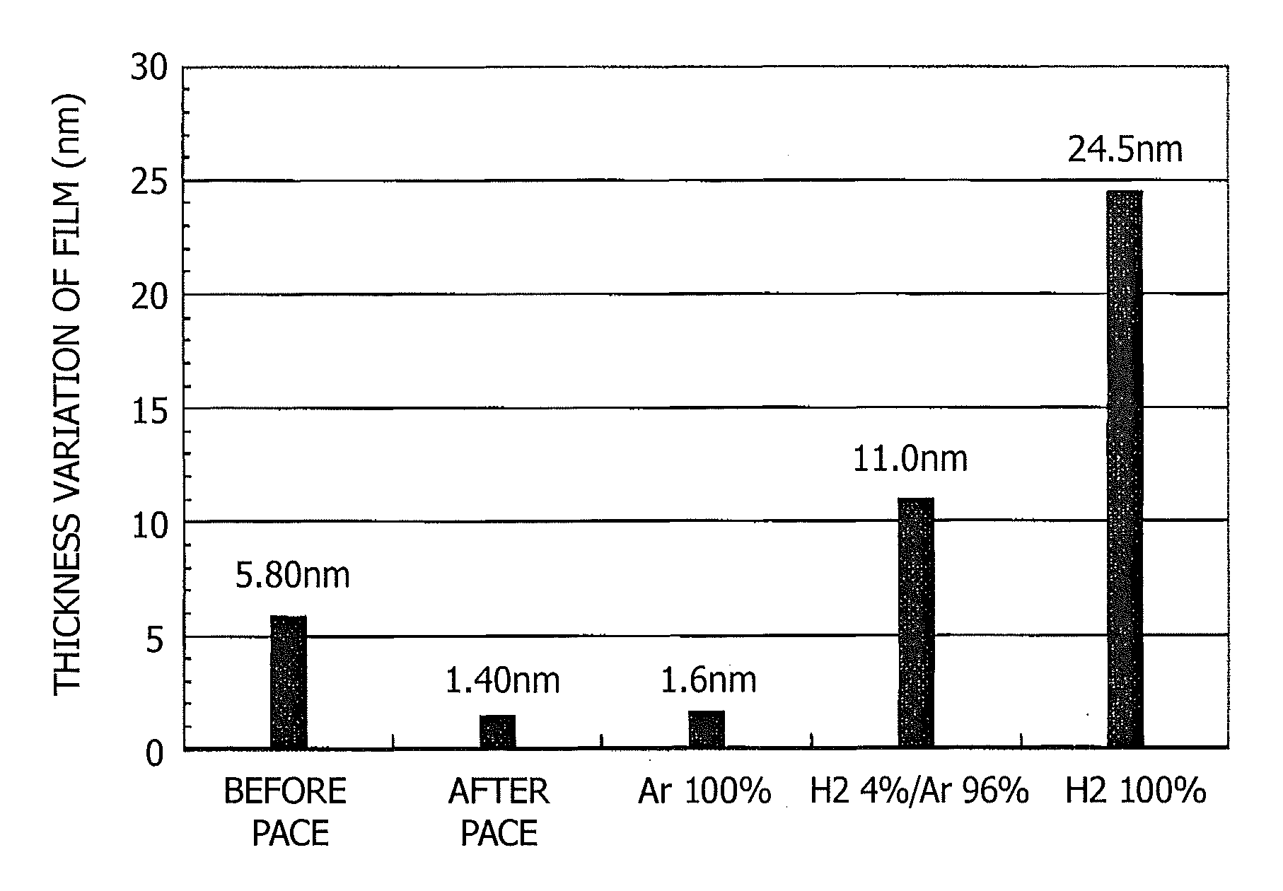
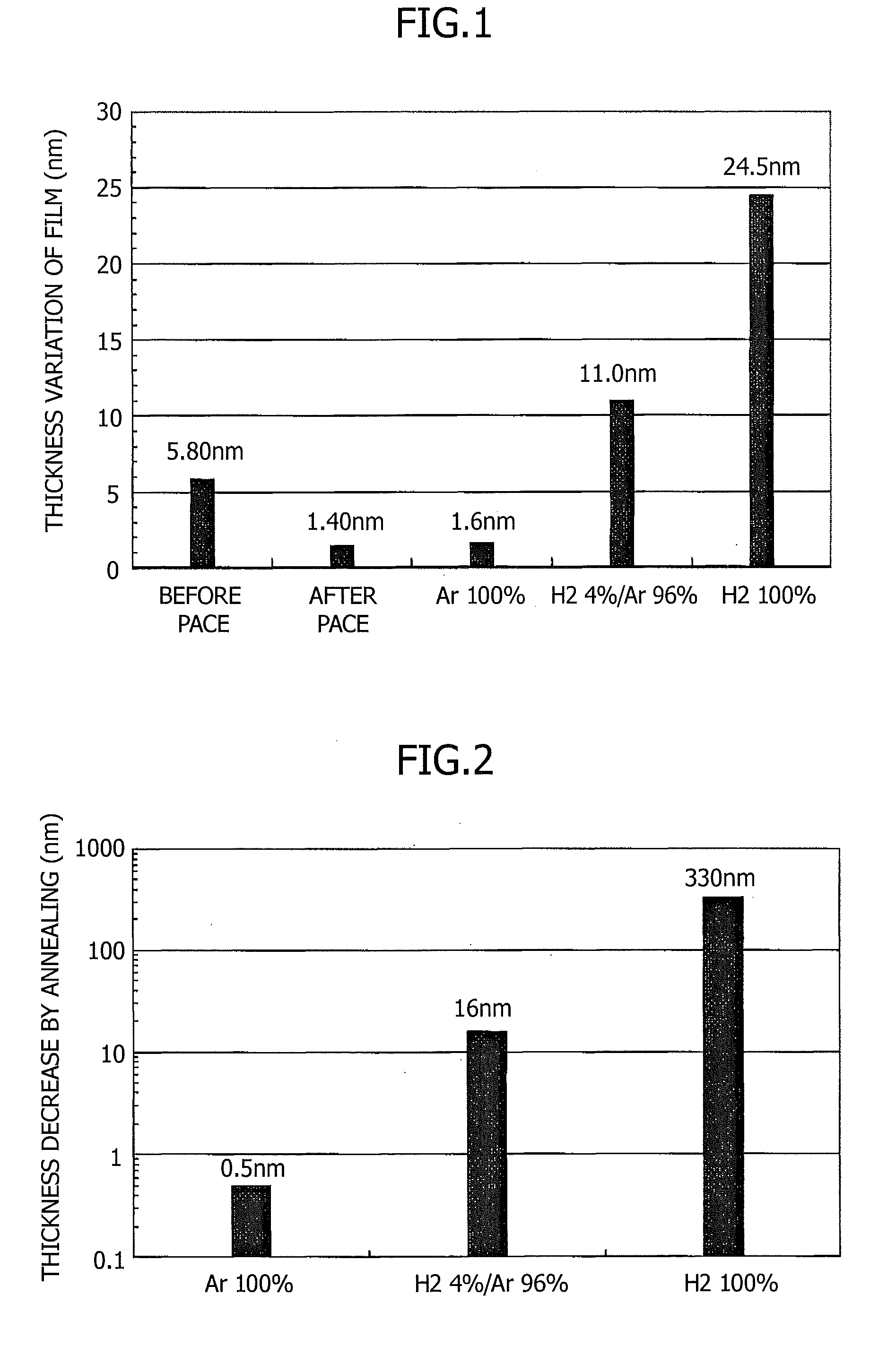
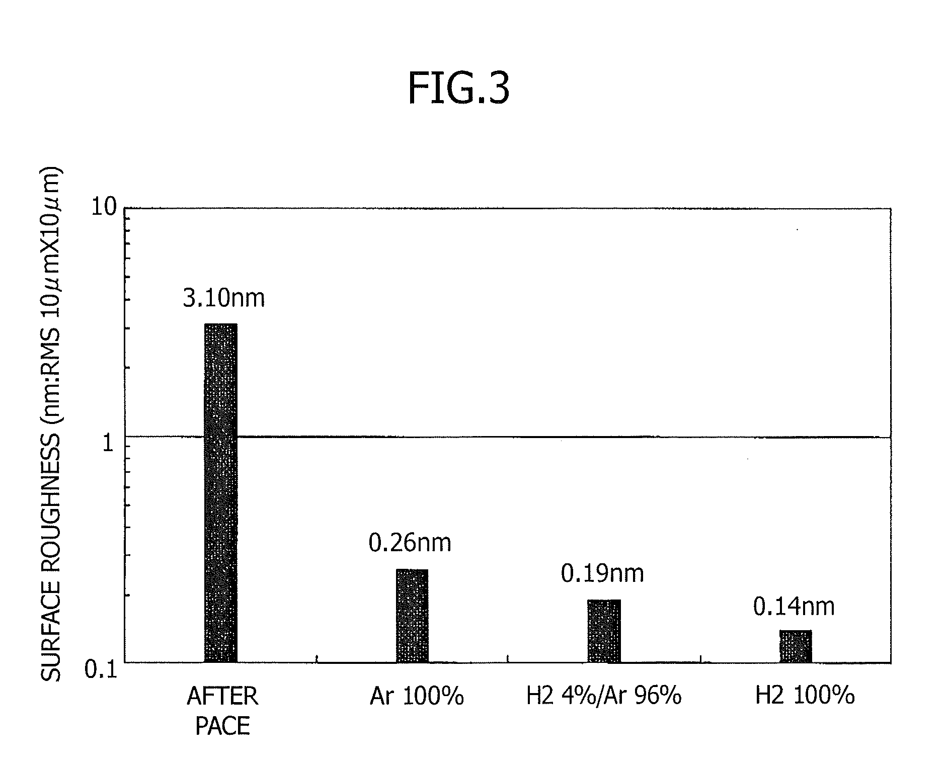
[0066]This example was implemented in the same way as in Example 1, provided that the anneal step (step c) was carried out in argon atmosphere containing 4 vol % of hydrogen. In this case, the decrease in film thickness (etching amount) for the SOI substrate was 16 nm, the surface roughness was 0.19 nm in terms of RMS, and the in-plane thickness variation of film was 11.0 nm.

[0067]As described above, the surface roughness of the SOI substrate was also RMS 0.3 nm or less in the case of the annealing in the argon atmosphere containing 4 vol % of hydrogen.


PUM

PropertyMeasurementUnit
temperatureaaaaaaaaaa
surface roughnessaaaaaaaaaa

Abstract

A method for minimizing thickness variation of a substrate in an anneal step and achieving the smoothing of the surface of the substrate. Specifically provided is a method for treating the surface of a SOI substrate, including the steps of treating the surface of the SOI substrate by the PACE method using a plasma or the GCIB method using a gas cluster ion beam and subjecting the treated substrate to a heat treatment in argon atmosphere or an inert gas atmosphere containing 4 vol % or less of hydrogen so that the treated SOI substrate can be annealed.

Description

TECHNICAL FIELD[0001]The present invention relates to a method for treating a surface of a SOI substrate.BACKGROUND ART[0002]Silicon-On-Insulator (SOI) wafers have been widely used in order to reduce parasitic capacitances and achieve higher speed devices. In recent years, the demand for thin film SOIs with an SOI layer (silicon layer) of 100 nm or less has been increased for the purpose of forming completely depleted layer type SOI devices. This is because higher speed devices can be expected from thinner SOI layers. For the thin film SOI wafer, the in-plane film thickness profile of the silicon layer is an extremely important factor, and the in-plane uniformity in nanometer-scale is required.[0003]However, it is practically difficult to achieve the nanometer-scale accuracy with a high yield, and it is difficult to make an improvement as it now stands.[0004]As a method for fabricating a thin film SOI with high in-plane uniformity in film thickness, a so-called PACE (Plasma Assisted...

Claims


Application Information

Patent Timeline
Patent Type & Authority Applications(United States)
IPC IPC(8): H01L21/02
CPCH01L21/3065H01L21/324H01L29/78603H01L21/76254H01L21/3247
Inventor AKIYAMA, SHOJIKUBOTA, YOSHIHIROITO, ATSUOTANAKA, KOUICHIKAWAI, MAKOTOTOBISAKA, YUJITAMURA, HIROSHI
Owner SHIN ETSU CHEM IND CO LTD
Why Eureka
Try Eureka