Semiconductor memory device and method for fabricating the same

a semiconductor memory and semiconductor technology, applied in the direction of semiconductor devices, basic electric elements, electrical appliances, etc., can solve the problems of reduced operational margin of sense amplifiers, increased electric field at storage nodes (sn) junctions, and reduced induced barrier, so as to suppress the short channel effect and parasitic capacitance, the effect of reducing the occurrence of gidl

Inactive Publication Date: 2011-01-27
SK HYNIX INC
View PDF7 Cites 23 Cited by
  • Summary
  • Abstract
  • Description
  • Claims
  • Application Information

AI Technical Summary

Benefits of technology

[0018]Embodiments of the present invention are directed to a semiconductor memory device and a fabricating method of the same capable of reducing the GIDL occurrence by forming an insulating film between the buried gate and the source and drain regions. The benefits include suppressing the short channel effect and the parasitic capacitance generated in the highly integrated semiconductor device.

Problems solved by technology

As a result, the short channel effect, the drain induced barrier lowering (DIBL) and other undesirable phenomena associated with small sized devices were observed in the conventional transistor.
However, as the design rule reaches below 100 nm, the method of increasing the channel doping concentration results in another problem, i.e., the electric field at a storage node (SN) junction is increased.
Because parasitic capacitance generated due to the short channel has also increased, the operational margin of the sense amplifier has been diminished, degrading the operational stability of the semiconductor memory device.
The simplest way to reduce parasitic capacitance is to increase the distance between the recess gate and the contact plug for a word line or a bit line; however, this would result in a larger unit cell size which runs contrary to the goal of providing highly integrated semiconductor devices.
As an overlap between the storage node contact region and the gate becomes wider and the electric field on the gate oxide film is increased, a gate-induced-drain-leakage (GIDL) is increased, thus deteriorating the refresh properties of the semiconductor memory device.

Method used


Image

  • Semiconductor memory device and method for fabricating the same
  • Semiconductor memory device and method for fabricating the same
  • Semiconductor memory device and method for fabricating the same

Examples


Embodiment Construction

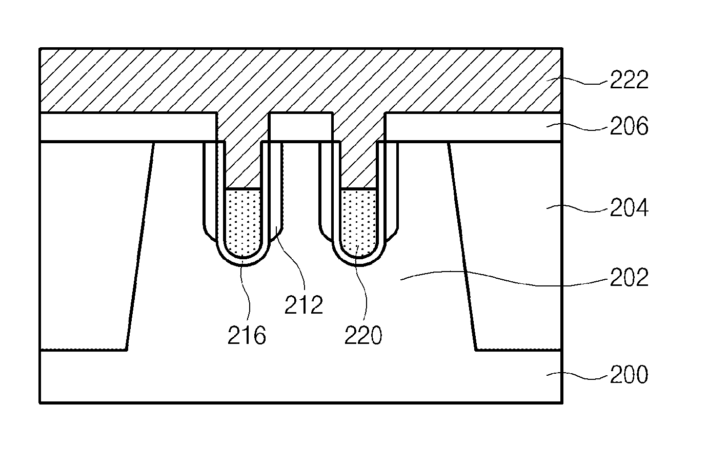
[0035]The present invention is directed to a semiconductor device including a buried gate structure. One embodiment of the present invention is directed to lowering parasitic capacitance. Since the buried gate is formed only at a lower part of a recess, a physical distance between a source / drain contact connected to either a source (capacitor) or a drain (bit line) and the buried gate can be increased so that the parasitic capacitance can be greatly reduced. However, a cross section size of the buried gate filling in a lower part of the recess is smaller in comparison with the recess gate filling in the whole recess. Therefore, it is preferable to use metal material instead of polysilicon as a conductive material constituting the buried gate.

[0036]Recently, a metal gate has been used instead of N+ poly-gate for forming the buried gate structure; however, a work function of the metal gate is higher than that of the N+ poly-gate so that a stronger electric field is applied to a gate o...


PUM


Abstract

A manufacturing method of a semiconductor device comprises forming a semiconductor substrate including an active region and an element isolation film, forming a first recess on the semiconductor substrate, forming an oxide film on a sidewall of the first recess, forming a second recess by etching a lower part of the first recess, and forming a gate in a lower part of the second recess.

Description

CROSS-REFERENCE TO RELATED APPLICATION[0001]The priority based on Korean patent application No. 10-2009-0067919 filed on Jul. 24, 2009, the disclosure of which is hereby incorporated in its entirety by reference, is claimed.BACKGROUND OF THE INVENTION[0002]The present invention relates to a fabricating method of a high integrated semiconductor memory device, and more specifically, to a stably operable semiconductor memory device having a buried gate structure and a fabricating method of the same.[0003]A semiconductor memory device includes a plurality of unit cells, each of which includes a capacitor and a transistor. The capacitor is used for temporarily storing data, and the transistor is used for transferring the data between a bit line and the capacitor in response to a control signal (word line) using properties of a semiconductor, i.e., a change of an electric conductivity in a channel region according to conditions such as an electric field. The transistor has three regions, ...

Claims


Application Information

Patent Timeline
Patent Type & Authority Applications(United States)
IPC IPC(8): H01L29/78H01L21/336
CPCH01L21/823437H01L21/823462H01L29/78H01L29/66621H01L29/4236H01L21/2255H01L29/66348
Inventor KIM, JONG IL
Owner SK HYNIX INC
Why Eureka
Try Eureka