Photosensitized solar cell, production method thereof and photosensitized solar cell module

a solar cell and photosensitization technology, applied in the direction of pv power plants, sustainable manufacturing/processing, final product manufacturing, etc., can solve the problems of not being solved, high production cost of silicon substrate, and high production cost, so as to reduce weight, improve characteristics, and produce easily

Inactive Publication Date: 2011-02-03
SHARP KK
View PDF5 Cites 28 Cited by
  • Summary
  • Abstract
  • Description
  • Claims
  • Application Information

AI Technical Summary

Benefits of technology

[0019]The present invention has been made in view of the above-mentioned problems, and is intended to provide a photosensitized solar cell, which is capable of being placed outdoors, reduced in the weight and improved in characteristics, and can be produced easily, a production method thereof, and a photosensitized solar cell module.
[0023]The present invention produces the following effects.(1) A transparent conductive film does not exist on the light-receiving surface side of the porous semiconductor layer as an electric generating element, so that no light incidence loss due to the transparent conductive film is caused and the short-circuit current is increased to improve the conversion efficiency. In particular, in the case of using a photosensitization element (quantum dot) of an inorganic material containing at least one of Cd, Pb, Sb, In, Ga, S, Se and As, the light absorption wavelength of the quantum dot is from 250 nm to 300 nm, so that the short-circuit current is largely improved as compared with the case of using the conductive glass (TCO) substrate for transmitting the light on the longer-wavelength side than 300 nm.(2) The element is formed on the substrate at a non-light-receiving surface side in the structure of the present invention, so that various materials may be used for the translucent cover member at the light-receiving surface side. Therefore, in the case of placing the photosensitized solar cell (or the module thereof) on a roof of an ordinary house for outdoor placement (for a domestic power source), tempered glass may be used as the translucent cover member. Accordingly, unlike as shown in the conventional structure (refer to FIG. 7), tempered glass does not need to be separately placed on the light-receiving surface side of the substrate for forming the element, so that no light incidence loss due to two glass substrates is caused and the short-circuit current is mare increased to allow a reduction in the weight and a reduction in costs for the photosensitized solar cell (or the module thereof).(3) In the conventional structure (refer to FIG. 7), the catalyst layer is formed on the porous insulating layer, so that measures to prevent the catalyst material from attaching to the porous semiconductor layer need to be performed; however, the catalyst material is directly formed on the conductive substrate in the structure of the present invention (refer to FIGS. 1 and 4), so that any catalyst material may be used as long as it binds to the conductive substrate.(4) A substrate obtained by forming a metal film exhibiting no corrosiveness to an electrolytic solution, such as one made of titanium, nickel or tantalum on an inexpensive insulative substrate (such as a ceramic substrate) may be used as the conductive substrate instead of expensive FTO glass with a transparent conductive film formed on a glass substrate, so that a further reduction in costs for the photosensitized solar cell (or the module thereof) may be intended.

Problems solved by technology

However, the former has a problem that the production cost for the silicon substrate is high, while the latter has a problem that the production cost rises by reason of necessity to use many kinds of gases for semiconductor production and complicated devices.
Thus, efforts to reduce the cost per electric power generation output by achieving higher efficiency in photoelectric conversion have been made in either of the solar cells, but the above-mentioned problems have not been solved yet.
However, the basic structure of the dye-sensitized solar cell described in Patent Document 1 is a structure such that an electrolytic solution is injected between the electrodes of two glass substrates, so that trial manufacture of a small-area solar cell is possible but application to a large-area solar cell such as one having a size of one meter square is difficult.
As a result, a problem is caused that a fill factor (FF) and a short-circuit current in current-voltage characteristics during the photoelectric conversion are decreased and a photoelectric conversion efficiency is decreased.
In the dye-sensitized solar cells of Patent Documents 1 to 4, a conductive glass (TCO) substrate is used at a light incidence side, and reflection and absorption of light are caused in the glass and the transparent conductive layer, so that there is a problem that the amount of incident light into an electric power generation portion is lost.

Method used


Image

  • Photosensitized solar cell, production method thereof and photosensitized solar cell module
  • Photosensitized solar cell, production method thereof and photosensitized solar cell module
  • Photosensitized solar cell, production method thereof and photosensitized solar cell module

Examples


embodiment 1-1

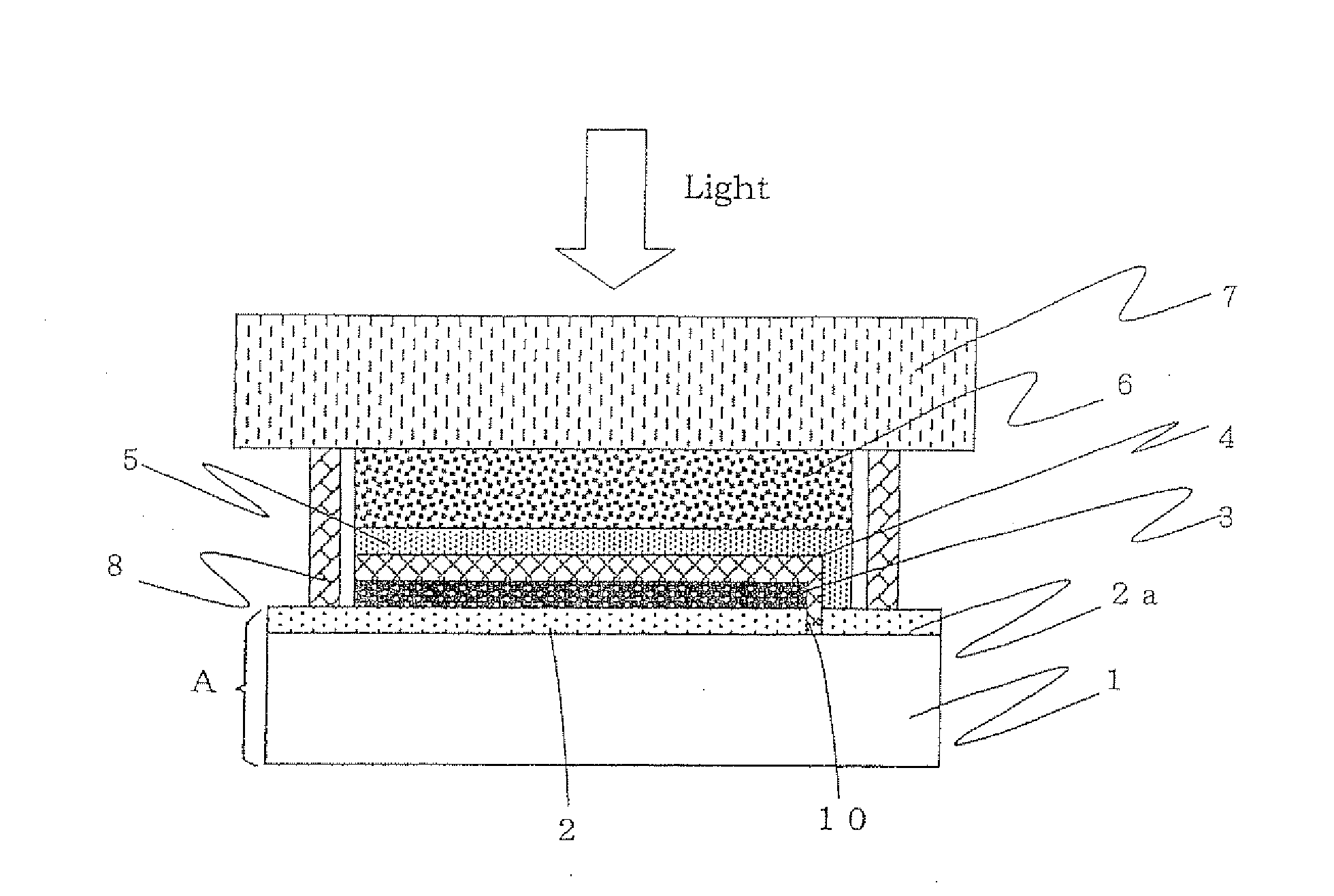
[0049]FIG. 1 is a schematic cross-sectional view showing Embodiment 1-1 of the photosensitized solar cell of the present invention. This photosensitized solar cell of Embodiment 1-1 (occasionally abbreviated as the solar cell hereinafter) is of a type having a conductive layer 5 between a porous insulating layer 4 and a porous semiconductor layer 6.

[0050]More specifically, this solar cell is provided with a conductive substrate A in which a conductive layer 2 (hereinafter referred to as the first conductive layer 2) is formed on a substrate 1, and a catalyst layer 3, the porous insulating layer 4, the conductive layer5 (hereinafter referred to as the second conductive layer 5), the porous semiconductor layer 6 with a photosensitizer adsorbed thereon and a translucent cover member 7, which are sequentially formed on the first conductive layer 2, and the porous insulating layer 4 and the porous semiconductor layer 6 contain an electrolyte. A sealing member 8 is provided on the outer c...

embodiment 1-2

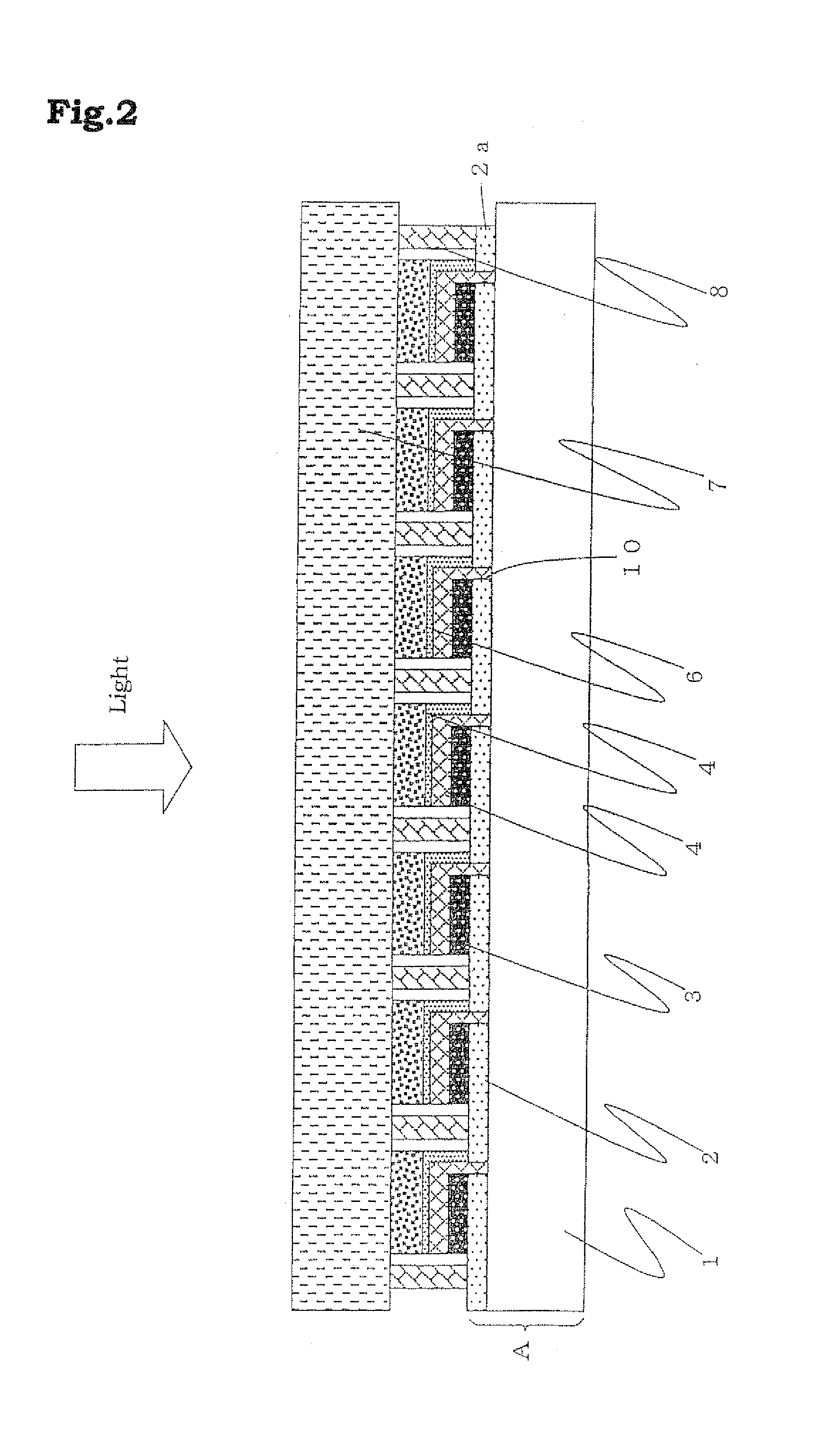
[0119]FIG. 2 is a schematic cross-sectional view showing a solar cell module in which a plurality of the solar cells of Embodiment 1-1 are electrically connected in series, and FIG. 3 is a schematic cross-sectional view showing a connecting portion of two solar cells in the solar cell module of FIG. 2. In FIGS. 2 and 3, the same reference numerals are given for the same components as the components in FIG. 1.

[0120]In producing this solar cell module, the conductive layer formed on the substrate 1 is first patterned at predetermined intervals by a laser scribe method to form a plurality of scribe lines with the conductive layer removed. Thus, the plural first conductive layers 2 electrically separated from one another are formed to offer a solar cell forming region on each of the first conductive layers 2.

[0121]Among the plural first conductive layers 2, the first conductive layer 2 at one end in a direction orthogonal to the scribe line is formed into a narrow width, on which first ...

embodiment 2-1

[0128]FIG. 4 is a schematic cross-sectional view showing Embodiment 2-1 of the photosensitized solar cell of the present invention. This photosensitized solar cell of Embodiment 2-1 is of a type with no conductive layers 5 between the porous insulating layer 4 and the porous semiconductor layer 6 in Embodiment 1-1. In FIG. 4, the same reference numerals are given for the same components as the components in FIG. 1.

[0129]Points of Embodiment 2-1 different from those of Embodiment 1-1 are mainly described hereinafter.

[0130]The solar cell of Embodiment 2-1 is primarily similar to that of Embodiment 1-1 except that the porous semiconductor layer 6 is formed from above the porous insulating layer 4 over the extraction electrode 2a. In Embodiment 2-1, the porous semiconductor layer 6 serves also as the second conductive layer in Embodiment 1-1, so that it is preferable that the electric resistance of the porous semiconductor layer 6 is low (about 40Ω / □ or less) or the length of the porous...


PUM


Abstract

A photosensitized solar cell characterized in that at least a catalyst layer 3, a porous insulating layer 4 internally containing an electrolyte, a porous semiconductor layer 6 with a photosensitizer adsorbed thereon, internally containing the electrolyte, and a translucent cover member 7 are laminated in this order on a conductive substrate.

Description

TECHNICAL FIELD[0001]The present invention relates to a photosensitized solar cell, a production method thereof and a photosensitized solar cell module. More specifically, the present invention relates to a photosensitized solar cell with improved characteristics and a reduced weight.BACKGROUND ART[0002]A solar cell for converting sunlight into an electric power has been attracting attention as an energy source replacing fossil fuel. Presently, solar cells using a crystalline silicon substrate and thin-film silicon solar cells have been put to practical use. However, the former has a problem that the production cost for the silicon substrate is high, while the latter has a problem that the production cost rises by reason of necessity to use many kinds of gases for semiconductor production and complicated devices. Thus, efforts to reduce the cost per electric power generation output by achieving higher efficiency in photoelectric conversion have been made in either of the solar cells...

Claims


Application Information

Patent Timeline
Patent Type & Authority Applications(United States)
IPC IPC(8): H01L31/05H01L31/02
CPCH01G9/2031H01G9/2059Y02E10/542Y02B10/12H01G9/2081Y02B10/10Y02P70/50
Inventor FUKUI, ATSUSHIFUKE, NOBUHIROYAMANAKA, RYOHSUKEHAN, LIYUAN
Owner SHARP KK
Why Eureka
Try Eureka