Large scale nanoelement assembly method for making nanoscale circuit interconnects and diodes

a nanoelement and assembly method technology, applied in the field of single walled carbon nanotubes, can solve the problems of lack of scalability needed for high-rate manufacturing methods previously availabl

Inactive Publication Date: 2011-02-03
NORTHEASTERN UNIV
View PDF1 Cites 38 Cited by
  • Summary
  • Abstract
  • Description
  • Claims
  • Application Information

AI Technical Summary

Problems solved by technology

A key challenge in utilizing SWNT and other nanoelements in nanoscale electronics is to develop their application in large scale devices.
However, previously available methods lack the scalability needed for high-rate manufacturing.

Method used


Image

  • Large scale nanoelement assembly method for making nanoscale circuit interconnects and diodes
  • Large scale nanoelement assembly method for making nanoscale circuit interconnects and diodes
  • Large scale nanoelement assembly method for making nanoscale circuit interconnects and diodes

Examples


example 1

Preparation of a Nanoporous Alumina Template

Porous alumina nanotemplates were prepared on 0.1×0.1 cm2 n-doped Si substrates (3-7 Ωcm). 1 μm thick Al was deposited by e-beam deposition on Si. Ordered nanoporous alumina templates were prepared by two step anodization (Matsuda et al., Li et al.) of the Al surface on the Si chip in 5 wt % oxalic acid. Anodization was carried out at 5 C under a constant 40 V DC potential until the whole Al layer was consumed (approx. 12 min). The resulting aluminum oxide barrier layer was removed by soaking in 5 wt % phorphoric acid for 40 min. The process produced a periodic, hexagonally-ordered nanoporous layer with pore diameter about 40 nm and thickness around 1 μm. The total area of alumina array was 0.4 cm2.

example 2

Preparation of a Three-Dimensional Assembly of SWNT

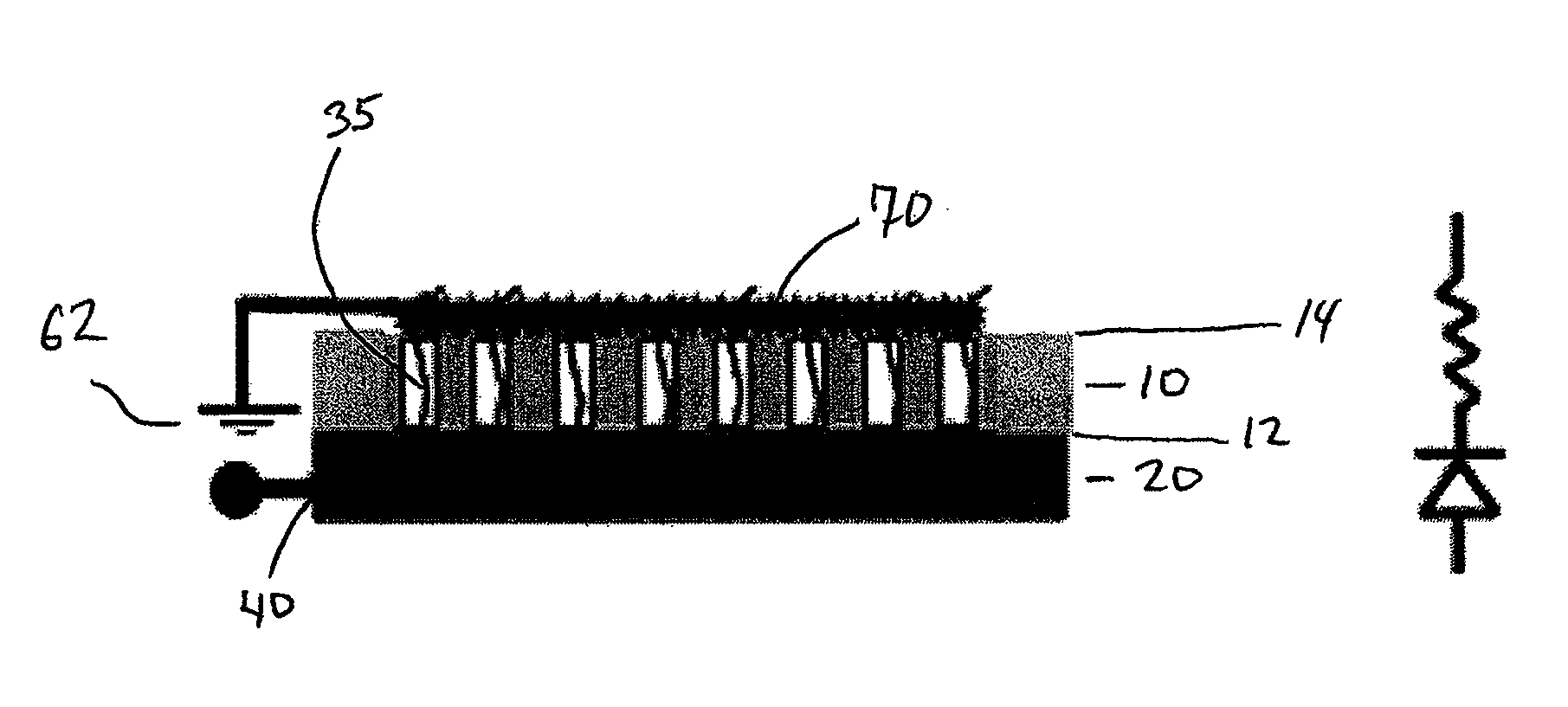
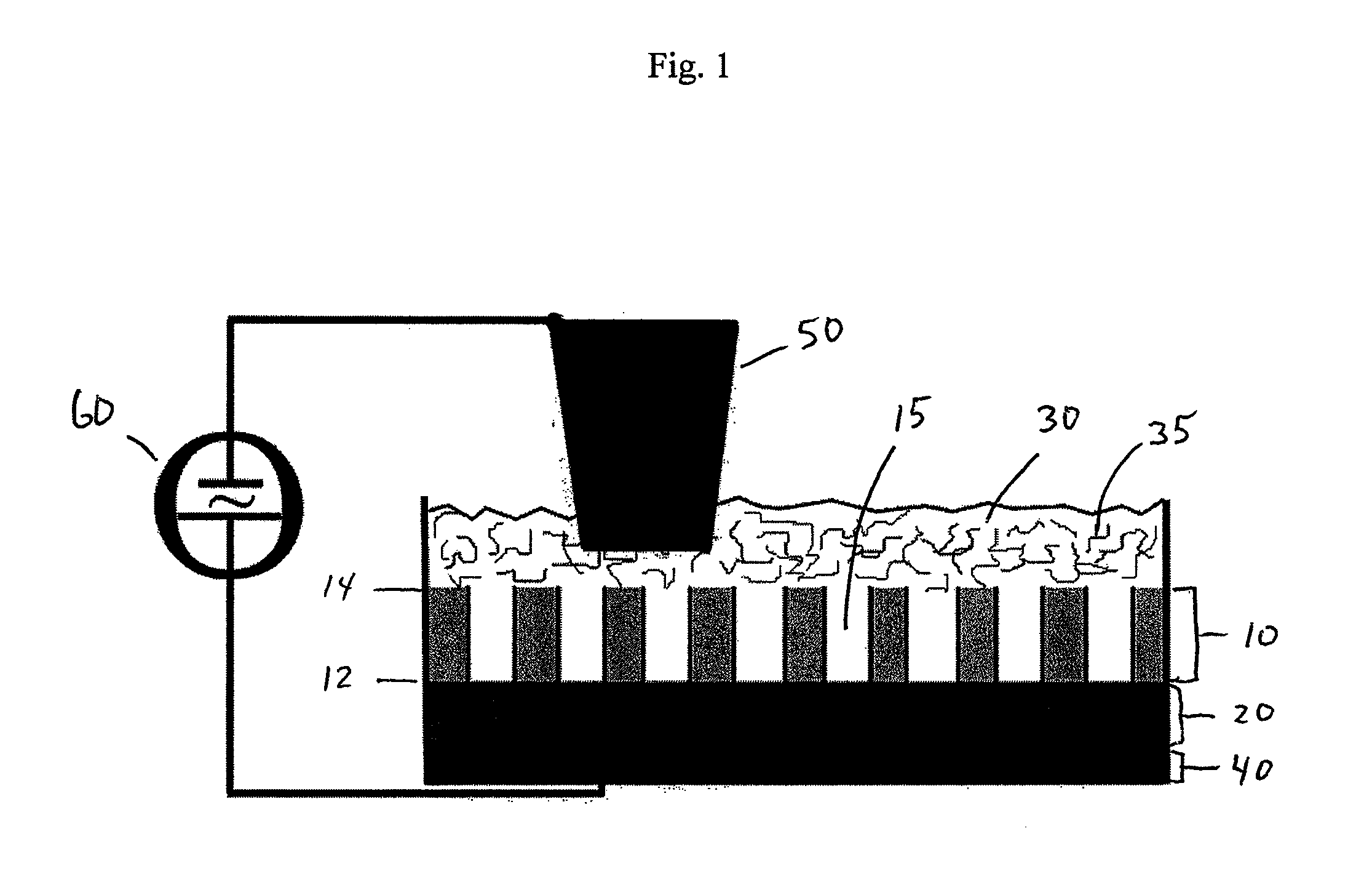
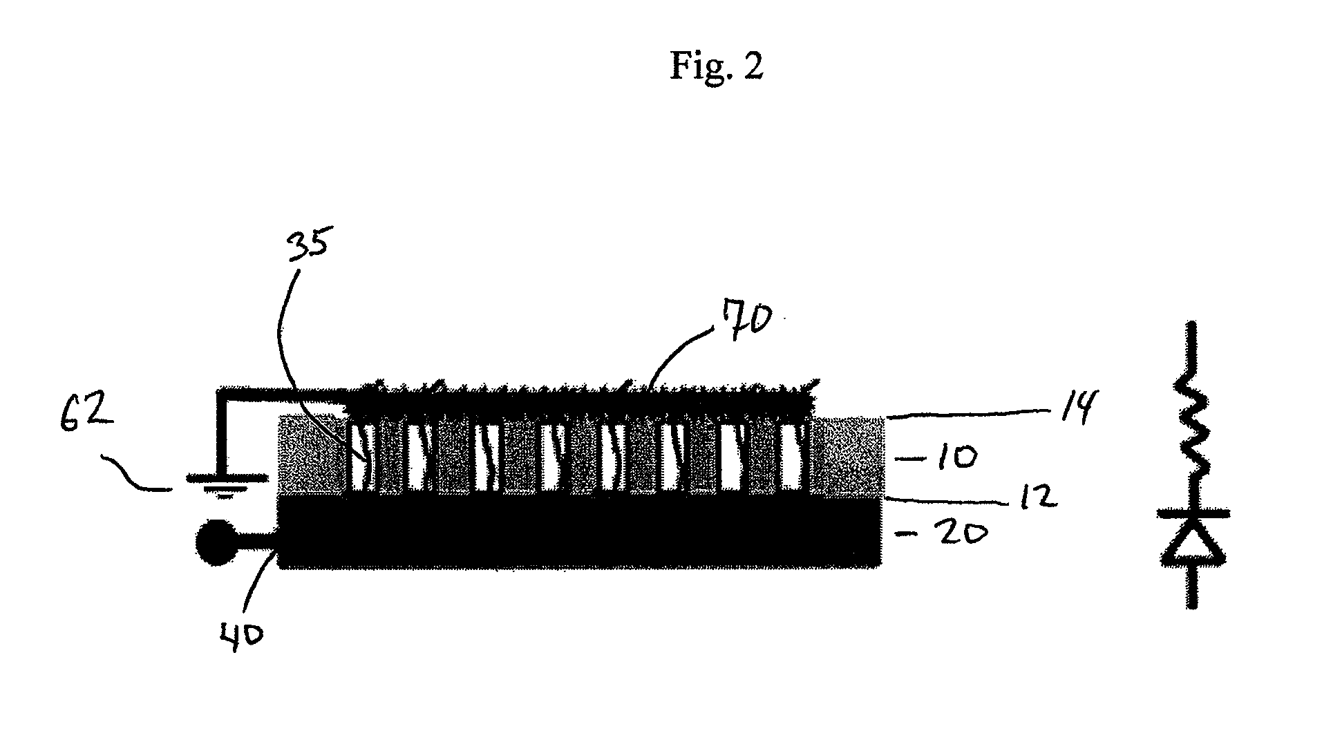
Negatively charged SWNT (Nantero, MA) were used for assembly into an alumina template prepared as described in Example 1. The SWNT solution was prepared in ethanol, and assembly occurred under 10V DC together with 10V AC at 10 MHz. A schematic of the assembly process can be seen in FIG. 1. The counter electrode was moved constantly to achieve assembly over large surface areas.

A pointed wire counter electrode was used for the assembly. This form of counter electrode can approach the template much closer, and the resulting electric field magnitude consequently is larger. The non-uniformity of the electric field is another reason for choosing a pointed electrode.

example 3

Characterization of a Three-Dimensional Assembly of SWNT

The SWNT assembly from Example 2 was studied using scanning electron microscopy (SEM) and its current-voltage relationship was determined.

The SEM images of the assembly (FIG. 3) show that SWNT migrated into the holes. The SWNT also stayed partly on the surface since the length of SWNT was much larger than the template thickness. Although the size of individual SWNT is too small to be visible under SEM, it was possible to see SWNT bundles as shown at FIG. 3.

Since SEM was not an optimal technique for investigating the quality of the assembly, the current passing between the top and bottom layer of the assembly through assembled SWNT was also measured (FIG. 4A). The upper surface of the alumina template was sputtered with a 15 nm thick Au layer to form an electrical connection between all the SWNT on the surface. The I-V measurement was carried out using a parameter analyzer with a probe station by attaching one electrode to the A...


PUM

PropertyMeasurementUnit
surface areaaaaaaaaaaa
conductivityaaaaaaaaaa

Abstract

Nanoelements such as single walled carbon nanotubes are assembled in three dimensions into a nanoscale template on a substrate by means of electrophoresis and dielectrophoresis at ambient temperature. The current-voltage relation indicates that strong substrate-nanotube interconnects carrying mA currents are established inside the template pores. The method is suitable for large-scale, rapid, three-dimensional assembly of 1,000,000 nanotubes per square centimeter area using mild conditions. Circuit interconnects made by the method can be used for nanoscale electronics applications.

Description

BACKGROUND OF THE INVENTIONSingle walled carbon nanotubes (SWNT) have attracted a great deal of attention for applications in nanoscale electronics. They have tremendous importance as interconnects, since conventional conductors (e.g., copper wires) fail to meet the required resistivity for smaller diameters (Cho et al.). Recent discoveries have demonstrated that SWNT have a large current capacity, as high as 109 A cm−2 (Yao et al.), or a mobility as high as 100,000 cm2 / Vs (Durkop et al.).A key challenge in utilizing SWNT and other nanoelements in nanoscale electronics is to develop their application in large scale devices. Available approaches in SWNT-related manufacturing are mainly divided into two types: growing SWNT into a device, and assembling prefabricated SWNT into a device. All methods of growing SWNT require high temperature synthesis (Bethune et al., Kong et al.), and in most methods nanotubes need a post process for cleaning, cutting and sorting to reach a narrow size d...

Claims


Application Information

Patent Timeline
Patent Type & Authority Applications(United States)
IPC IPC(8): H01L29/66H01L21/3205C25B7/00B82Y40/00
CPCB81B2207/07B81C1/00031B81C2201/0183B82Y10/00Y02E10/549H01L51/0006H01L51/0048H01L51/057G11C13/025Y02P70/50H10K71/125H10K85/221H10K10/491
Inventor SRIDHAR, SRINIVASGULTEPE, EVINNAGESHA, DATTATRI
Owner NORTHEASTERN UNIV
Why Eureka
Try Eureka