Organic Thin Film Transistors and Methods of Making the Same

Active Publication Date: 2011-02-03
CAMBRIDGE DISPLAY TECH LTD
View PDF4 Cites 12 Cited by
  • Summary
  • Abstract
  • Description
  • Claims
  • Application Information

AI Technical Summary

Benefits of technology

[0032]For a bottom-gate device an organic dielectric material may be utilized to provide a large differential in the chemical properties of the dielectric layer and the source and drain electrodes such that selective binding of the dopant moiety to the source and drain electrodes is encouraged

Problems solved by technology

One of the challenges with all organic thin film transistors is to ensure a good ohmic contact between the source and drain electrodes and the organic semiconductor (OSC).
One problem with the aforementioned arrangement is that a relatively small number of materials will have a work function which has a good match energy level match with the HOMO/LUMO of the OSC.
Many of these materials may be expensive, such as gold, and/or may be difficult to deposit to form the source and drain electrodes.
Furthermore, even if a suitabl

Method used


Image

  • Organic Thin Film Transistors and Methods of Making the Same
  • Organic Thin Film Transistors and Methods of Making the Same
  • Organic Thin Film Transistors and Methods of Making the Same

Examples


Example

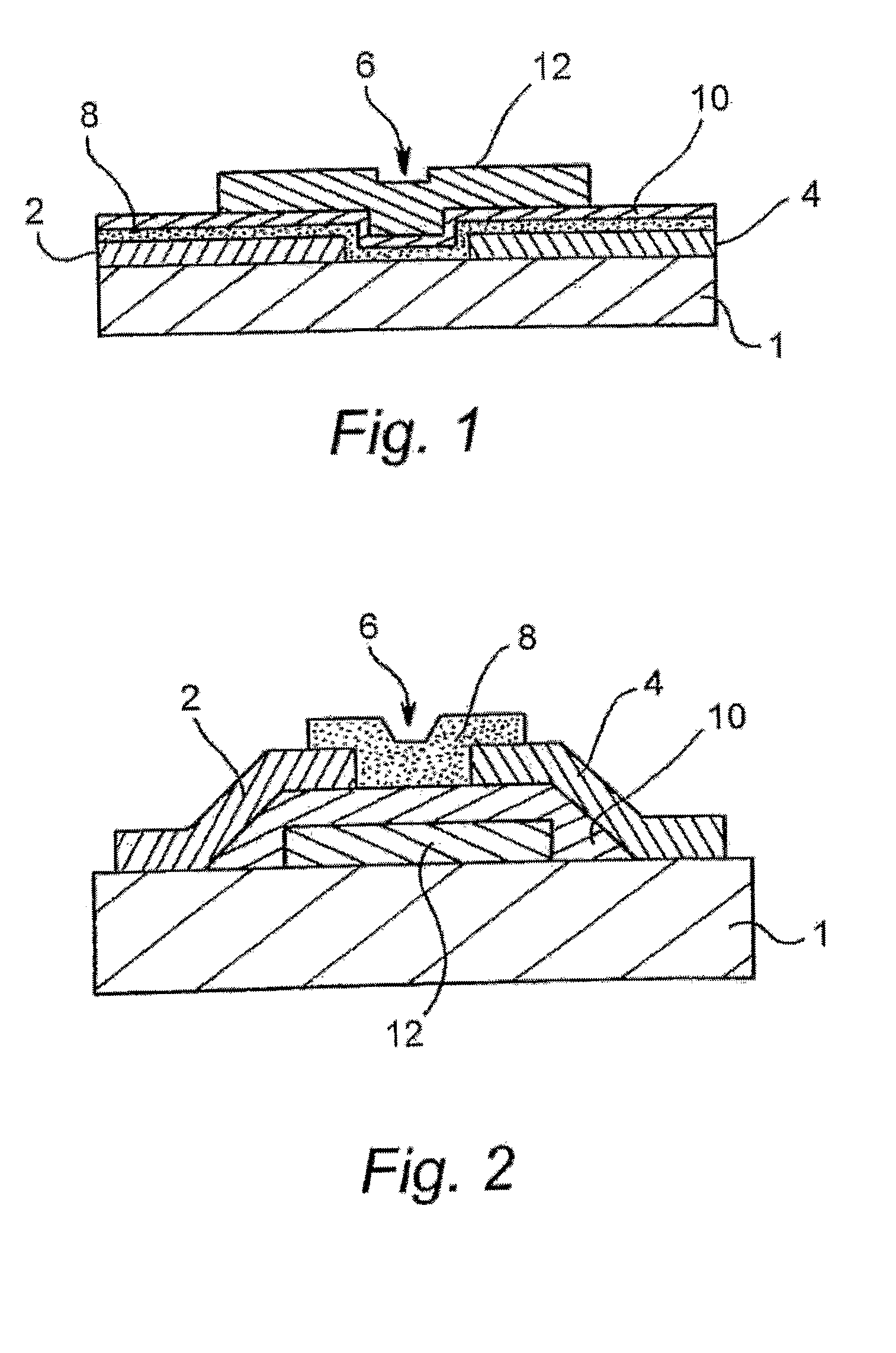
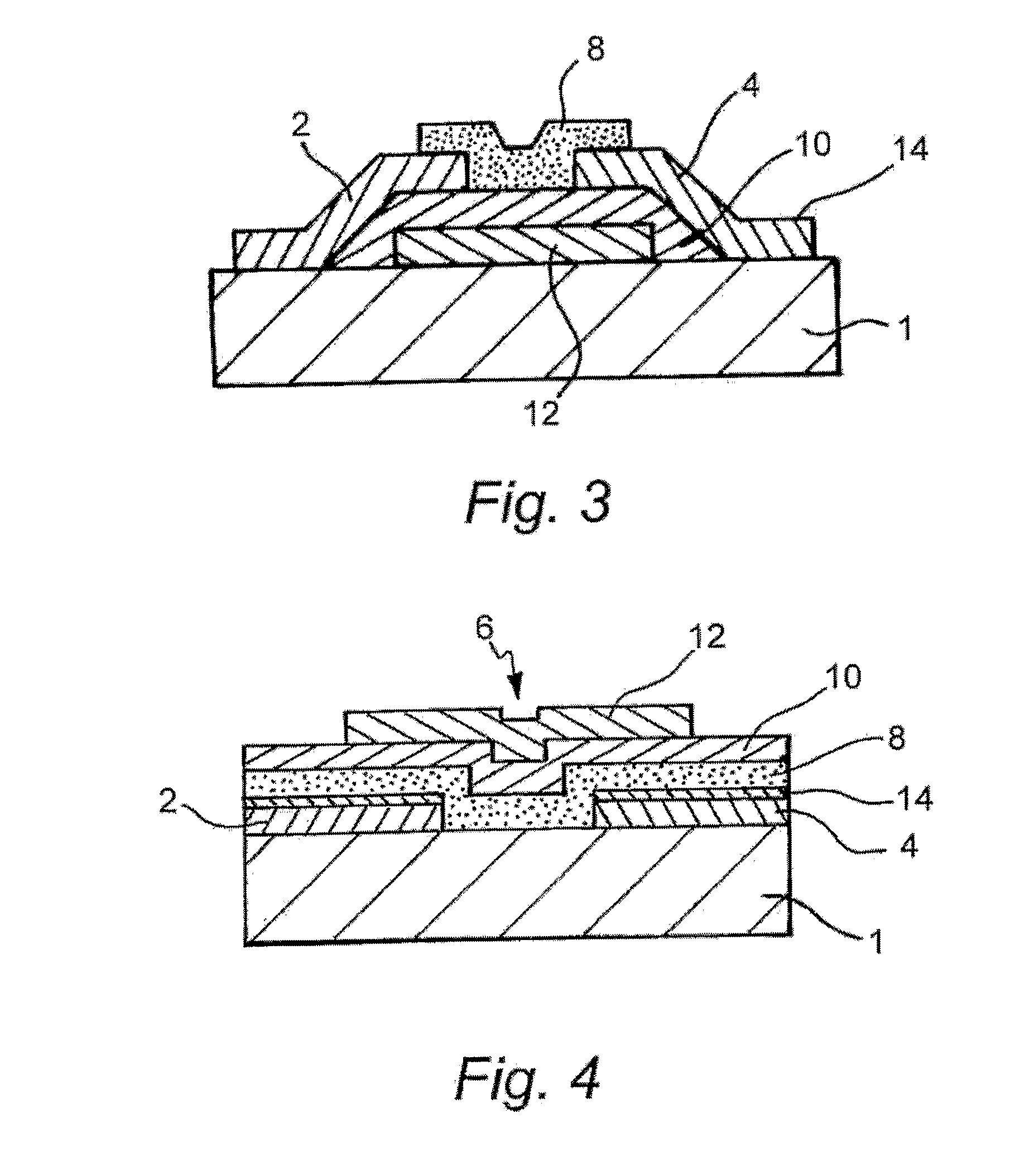
[0046]FIG. 3 shows a bottom-gate organic thin film transistor according to an embodiment of the present invention. The structure is similar to the prior art arrangement shown in FIG. 2 and for clarity like reference numerals have been used for like parts. The key difference between the arrangement shown in FIG. 3 is that the source and drain electrodes 2, 4 have disposed thereon a thin self-assembled layer of a material 14 comprising a dopant moiety having a redox potential of at least 0.3 eV relative to a saturated calomel electrode (SCE) in acetonitrile.

[0047]FIG. 4 shows a top-gate organic thin film transistor according to an embodiment of the present invention. The structure is similar to the prior art arrangement shown in FIG. 1 and for clarity like reference numerals have been used for like parts. Again, the key difference between the arrangement shown in FIG. 4 is that the source and drain electrodes 2, 4 have disposed thereon a thin self-assembled layer of a material 14 comp...


PUM

PropertyMeasurementUnit
Electrical conductivityaaaaaaaaaa
Energyaaaaaaaaaa

Abstract

An organic thin film transistor, and a method of making the same, comprising a source and drain electrode and organic semi-conductive material disposed therebetween in a channel region, in which the source and drain electrodes have disposed on them a thin self-assembled layer of a material comprising a dopant moiety for chemically doping the organic semi-conductive material by accepting electrons, the dopant moiety having a redox potential of at least 0.3 eV relative to a saturated calomel electrode in acetonitrile.

Description

FIELD OF INVENTION[0001]Aspects of the present invention relate to organic thin film transistors and methods of making the same.BACKGROUND OF THE INVENTION[0002]Transistors can be divided into two main types: bipolar junction transistors and field-effect transistors. Both types share a common structure comprising three electrodes with a semi-conductive material disposed therebetween in a channel region. The three electrodes of a bipolar junction transistor are known as the emitter, collector and base, whereas in a field-effect transistor the three electrodes are known as the source, drain and gate. Bipolar junction transistors may be described as current-operated devices as the current between the emitter and collector is controlled by the current flowing between the base and emitter. In contrast, field-effect transistors may be described as voltage-operated devices as the current flowing between source and drain is controlled by the voltage between the gate and the source.[0003]Tra...

Claims


Application Information

Patent Timeline
IPC IPC(8): H01L51/05H01L51/40
CPCH01L51/002H01L51/0036H01L51/105H01L51/0541H01L51/0545H01L51/0039H10K71/30H10K85/115H10K85/113H10K10/464H10K10/84H10K10/466H10K19/10H10K59/12H10K85/111H10K85/1135H10K85/623H10K10/462
Inventor BURROUGHES, JEREMYMURPHY, CRAIGWHITING, GREGORYHALLS, JONATHAN
Owner CAMBRIDGE DISPLAY TECH LTD
Why Eureka
Try Eureka