SRAM cell and SRAM device

Inactive Publication Date: 2011-02-03
NAT INST OF ADVANCED IND SCI & TECH
View PDF1 Cites 4 Cited by
  • Summary
  • Abstract
  • Description
  • Claims
  • Application Information

AI Technical Summary

Benefits of technology

[0018]In FIGS. 6 and 7 corresponding to Patent Document 1, a wiring presents between M2 and M6 increases spacing between M3 and M4. In the SRAM cell according to the present invention, a space for wiring between the second and sixth n-channel FETs is preserved, and the cell area can be saved and the cell with an area of 128 F2 can be realized.

Problems solved by technology

However, in near future, it will become difficult to suppress the short channel effect in a bulk planar type MOS field effect transistor, which causes an increase of leakage current.
However, no consideration is taken in this SRAM cell from a view point of reducing standby power consumption.
In order to realize an SRAM cell using the four-terminal double gate FETs with smaller area and to realize a highly integrated SRAM device, this figure, however is not sufficient.

Method used


Image

  • SRAM cell and SRAM device
  • SRAM cell and SRAM device
  • SRAM cell and SRAM device

Examples


Embodiment Construction

[0026]Although configurations of a circuit and its peripheral circuit configuration disclosed in the present invention are the same as those disclosed in Patent Document 1 as shown in FIGS. 6 and 7, and the circuit works if the circuit disclosed in, for example, Patent Document 2 is adopted, the SRAM cell disclosed in the present invention has a structure as shown in, for example, FIGS. 1 to 4 which is different from that disclosed in Patent Document 1.

[0027]Detailed structure of the SRAM cell shown in FIGS. 1 to 4 is as follows.

[0028]FIG. 1 is a schematic diagram illustrating an arrangement method of six four-terminal double gate FETs (M1 to M6) configuring an SRAM cell.

[0029]The SRAM cell includes a first to fourth semiconductor thin plates standing on a single substrate and sequentially arranged parallel to each other. A first four-terminal double gate FET (M1) with a first conduction type and a second four-terminal double gate FET (M2) with a second conduction type are formed on...


PUM


Abstract

An 
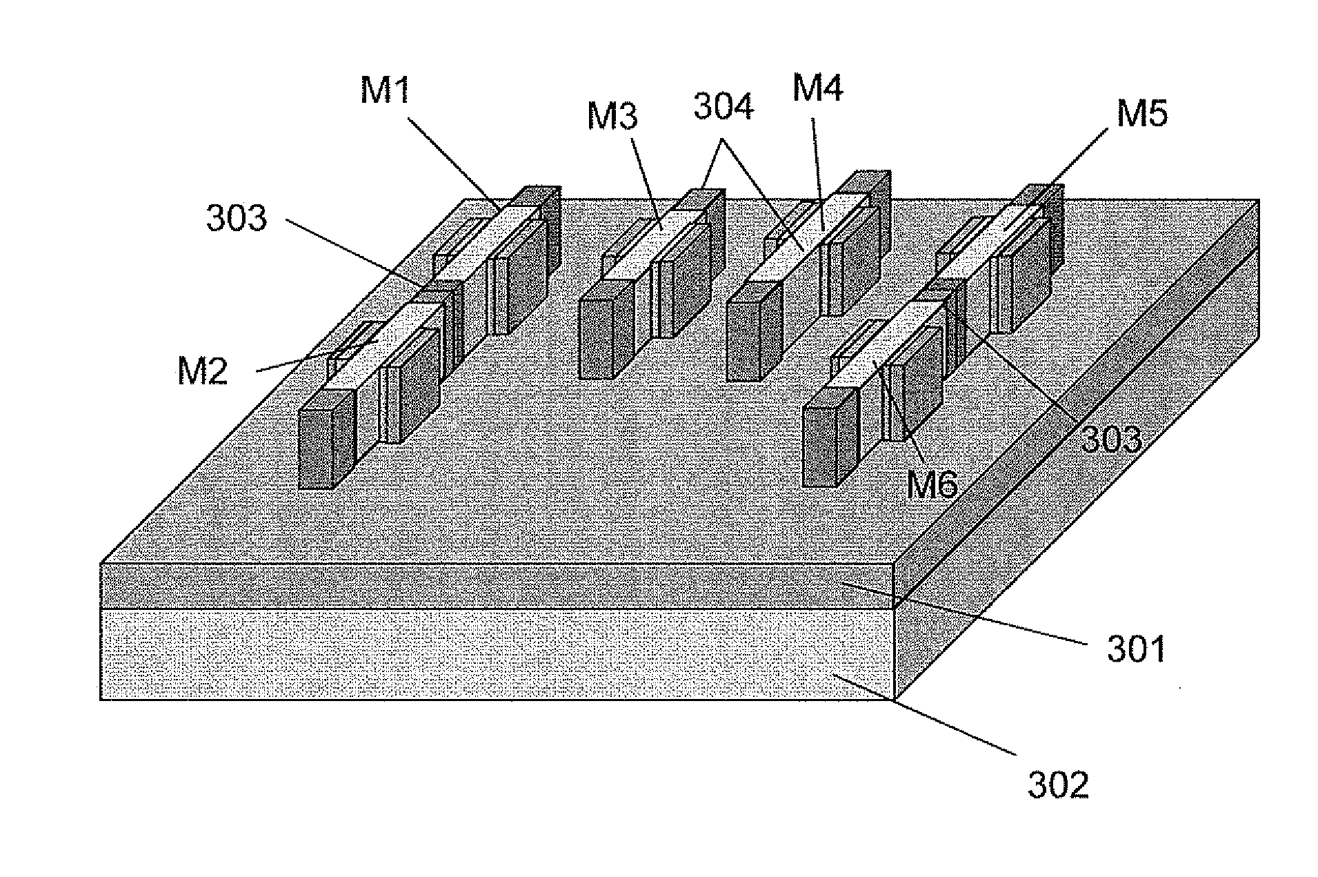
SRAM cell comprising a first to fourth semiconductor thin plates standing on a single substrate and sequentially arranged parallel to each other, on the first semiconductor thin plate a first four-terminal double gate FET with a first conduction type and a second four-terminal double gate FET with a second conduction type being formed and connected in series to each other, on the second semiconductor thin plate a third four-terminal double gate FET with the second 
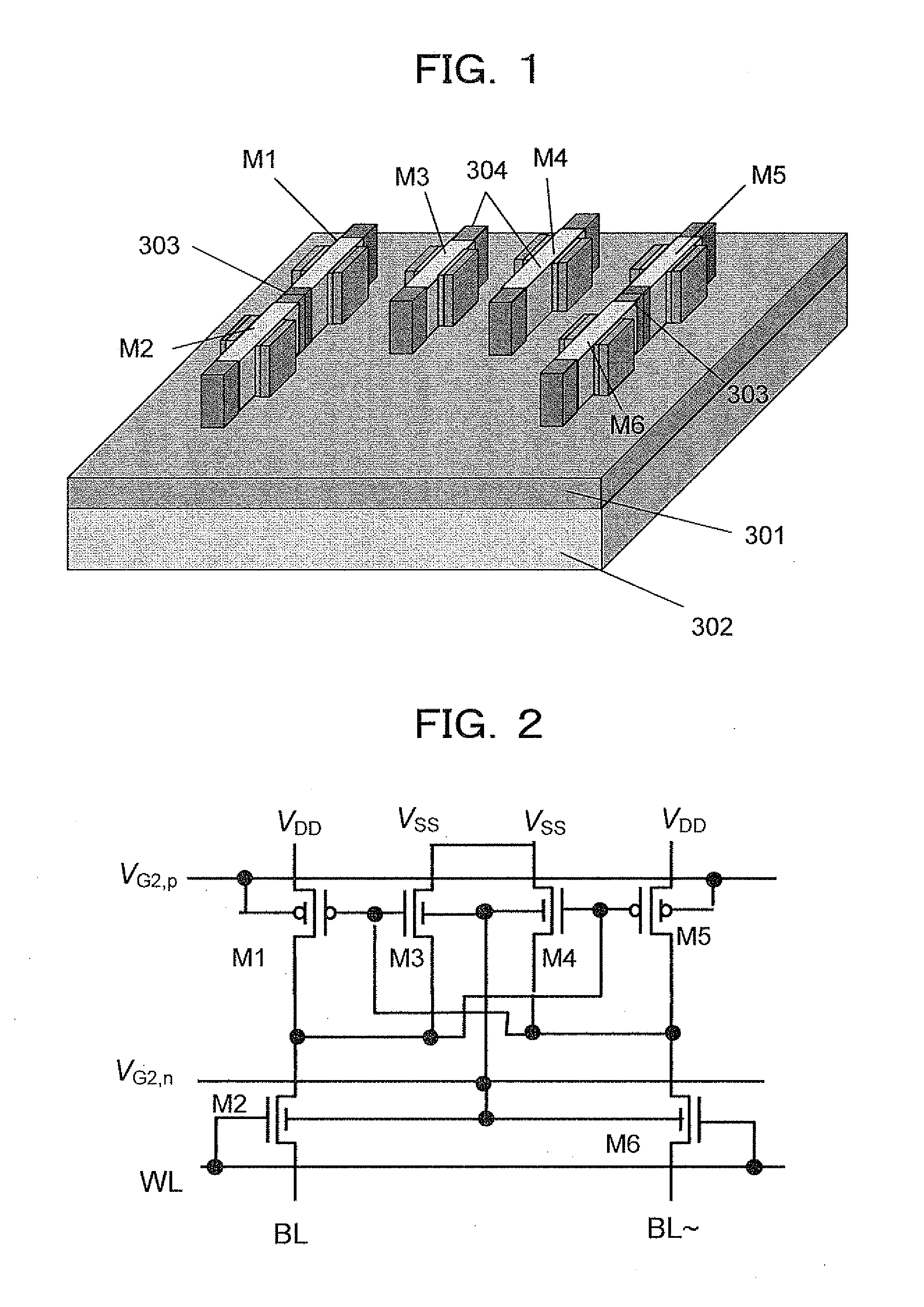
conduction type being formed, on the third semiconductor thin plate a fourth four-terminal double gate FET with the second conduction type is formed, on the fourth semiconductor thin plate a fifth four-terminal double gate FET with the first conduction type and a sixth four-terminal double gate FET with the second conduction type being formed and connected in series to each other. The second and sixth four-terminal double gate FETs constitute select transistors with logic signal input gates thereof being connected to a word line. The first and third four-terminal double gate FETs and the fourth and the fifth four-terminal double gate FETs respectively constitute cross-coupled complementary inverters to realize a flip-flop. The 
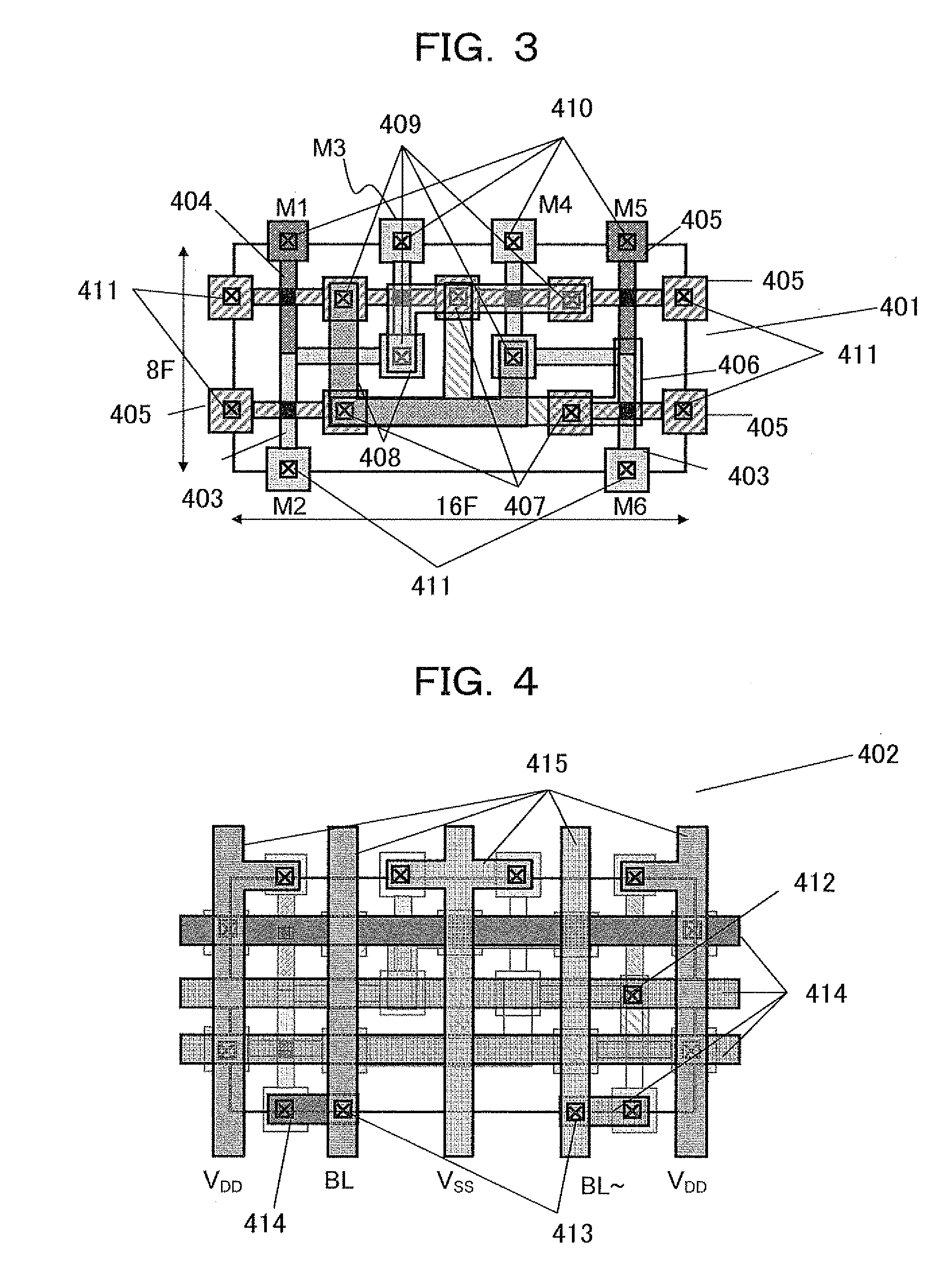
SRAM cell is characterized in that the first four-terminal double gate FET and the third four-terminal double gate FET are neighboring with each other and logic signal input gates thereof are formed on the side surfaces facing to each other of the respective semiconductor thin plates; the fourth four-terminal double gate FET and the fifth four-terminal double gate FET are neighboring with each other and logic input gates thereof are formed on the side surfaces facing to each other of the respective semiconductor thin plates; the third four-terminal double gate FET and the fourth four-terminal double gate FET are neighboring with each other and a threshold voltage control gates thereof are formed on the side surfaces facing to each other of the respective semiconductor thin plates; the second four-terminal double gate FET and the sixth four-terminal double gate FET are neighboring with each other sandwiching the second and third semiconductor thin plates and threshold voltage control gates thereof being formed on side surfaces facing to each other of the respective semiconductor thin plate; the threshold voltage control gates of the second, third, fourth, and sixth four-terminal double gate FETs are connected in common to a first bias wiring; threshold voltage control gates of the first and fifth four-terminal double gate FETs are connected in common to a second bias wiring; and the word line and the first and second bias wirings are arranged in a direction perpendicular to the alignment direction of the first to the fourth semiconductor thin plates.

Description

TECHNICAL FIELD[0001]The present invention relates to an SRAM (Static Random Access Memory) cell and an SRAM device.BACKGROUND ART[0002]Conventionally, an SRAM cell is fabricated by using a planar type MOS field effect transistor (Metal-Oxide-Silicon Field-Effect Transistor) on a bulk type or an SOI (Silicon On Insulator) silicon substrate. However, in near future, it will become difficult to suppress the short channel effect in a bulk planar type MOS field effect transistor, which causes an increase of leakage current. As a method to avoid this problem, Non-Patent Document 1 suggests fabricating an SRAM cell by using a four-terminal double gate FET (Field-Effect Transistor).[0003]This SRAM cell is realized with an area of 118 F2, where F denotes a half length of the pitch of the metallic wiring in the first layer. However, no consideration is taken in this SRAM cell from a view point of reducing standby power consumption. An SRAM cell circuit designed from a point of view of reduci...

Claims


Application Information

Patent Timeline
IPC IPC(8): H01L27/088
CPCH01L21/823821H01L27/0924H01L29/785H01L27/1211H01L27/1104H10B10/12
Inventor OUCHI, SHINICHI
Owner NAT INST OF ADVANCED IND SCI & TECH
Why Eureka
Try Eureka