Wafer imaging and processing method and apparatus

a processing method and wafer technology, applied in image enhancement, semiconductor/solid-state device testing/measurement, instruments, etc., can solve the problems of limited two-dimensional information about lateral variations of material quality within each wafer obtained, limiting the time available for characterisation, and limiting the time available for in-line characterisation of each sample, so as to improve the quality of the solar cell

Inactive Publication Date: 2011-02-03
BT IMAGING PTY LTD
View PDF8 Cites 62 Cited by
  • Summary
  • Abstract
  • Description
  • Claims
  • Application Information

AI Technical Summary

Benefits of technology

[0033]The method can further include the step of: (d) utilising the results of the analysis step to alter parameters associated with a series of processing steps in the formation of a solar cell so as to improve the quality of the solar cell. The parameters can include the conditions for firing a metal pattern into the silicon wafer. The parameters can also include the diffusion conditions for diffusing materials into the silicon wafer.

Problems solved by technology

Normally, only limited two-dimensional information about lateral variations of the material quality within each wafer is obtained.
This is as a result of a high volume solar cell production line typically handling 1 wafer every one to three seconds, which limits the time available for characterisation.
The average throughput of a typical silicon solar cell production line may be one solar cell every one to three seconds, which limits the time available for in-line characterisation of each sample.
Existing spatially resolved measurements are generally too slow to yield high resolution two-dimensional information about the electronic wafer quality in such short timeframes.
On the other hand it is known that small defects can have a large impact on device performance.
Manufacturers thus have limited tools that allow them to characterise the electronic properties of every wafer or of even a large fraction of wafers going through a production process with sufficiently high lateral spatial resolution.
Dislocations are a common type of structural defect in semiconductors such as silicon, and their presence strongly affects the electronic properties of the materials and consequently the performance of devices such as solar cells manufactured from them.

Method used


Image

  • Wafer imaging and processing method and apparatus
  • Wafer imaging and processing method and apparatus
  • Wafer imaging and processing method and apparatus

Examples


Embodiment Construction

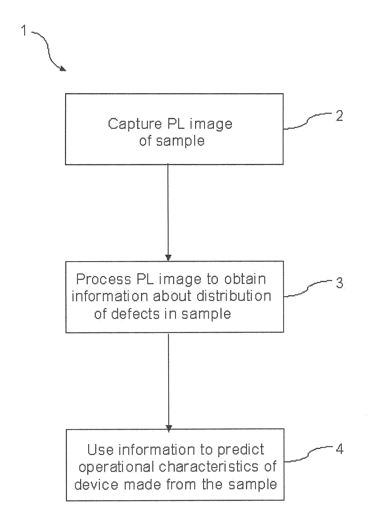
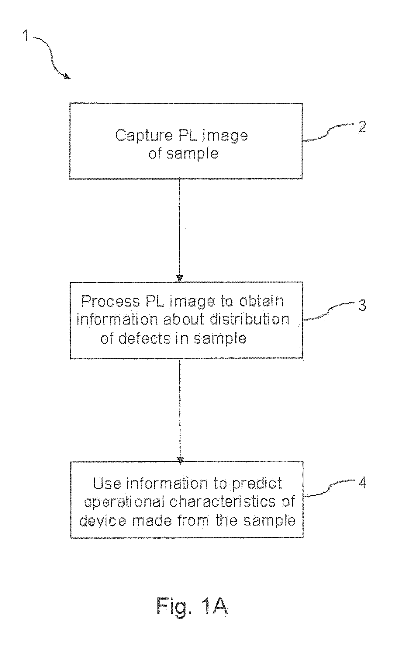
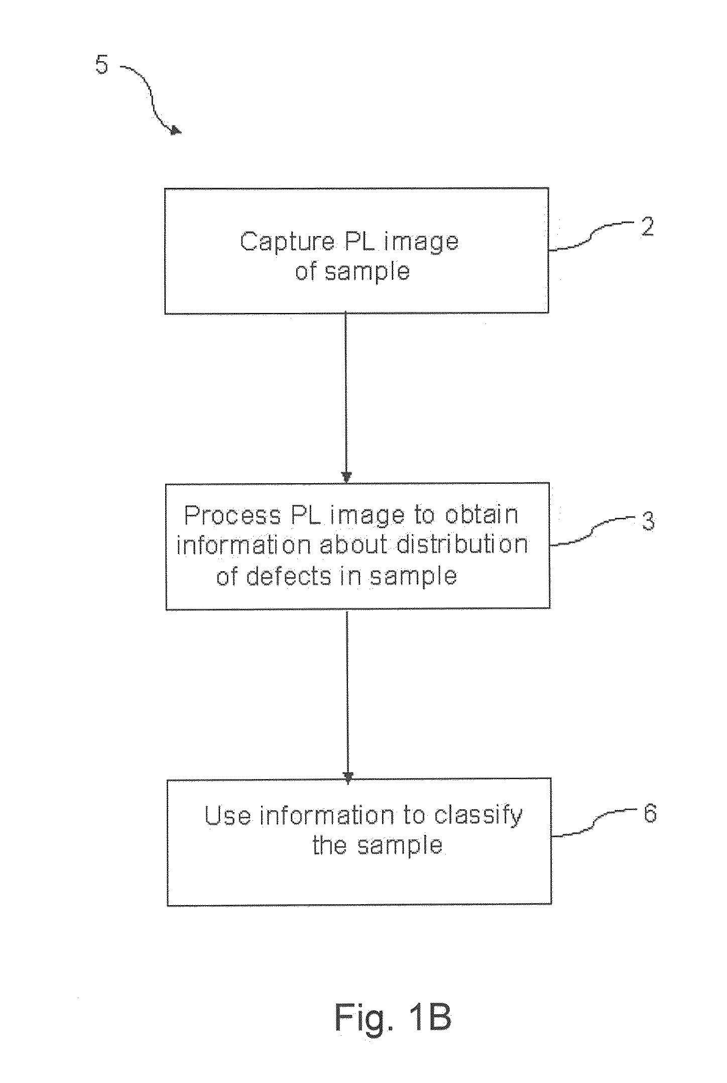
[0111]Lateral variations in the electronic material quality of the substrate material (for example a silicon wafer) can have a large impact on key performance parameters of solar cells manufactured from the material, such as open circuit voltage, short circuit current density, fill factor and efficiency.

[0112]The preferred embodiment provides methods and systems that can rapidly assess the quality of raw wafers at the start of solar cell manufacturing or at the end of wafer manufacturing and predict cell performance parameters or statistical variations thereof expected under normal processing conditions. The methods and systems can also be used to assess the effect of additional processing steps, such as annealing, intended to improve the electronic material quality.

[0113]The preferred embodiment includes analysis of photoluminescence (PL) images of a bandgap material, i.e. images of band-to-band recombination luminescence 15 generated by photo-excitation of the material. In alterna...


PUM


Abstract

A method (1) is disclosed whereby luminescence images are captured (2) from as-cut or partially processed bandgap materials such as multicrystalline silicon wafers. These images are then processed (3) to provide information about defects such as dislocations within the bandgap material. The resultant information is then utilised (4) to predict various key parameters of a solar cell manufactured from the bandgap material, such as open circuit voltage and short circuit current. The information may also be utilised to apply a classification to the bandgap material. The methods can also be used to adjust or assess the effect of additional processing steps, such as annealing, intended to reduce the density of defects in the bandgap materials.

Description

FIELD OF THE INVENTION[0001]The present invention relates to the field of processing luminescence images acquired from direct and indirect bandgap semiconductor materials such as silicon wafers. In particular it relates to methods and apparatus for analysing luminescence images of wafers to obtain information about defects in the wafer material. This information may be used to classify the wafers or to predict operational characteristics of devices made from them.BACKGROUND OF THE INVENTION[0002]Any discussion of the prior art throughout the specification should in no way be considered as an admission that such prior art is widely known or forms part of common general knowledge in the field.[0003]Most commercial photovoltaic cells (in particular solar cells) today are made from typically 10×10 cm2 up to 21×21 cm2 multicrystalline (mc) silicon wafers which are cut from a cast multicrystalline silicon block. The main processing steps on forming a solar cell after cutting the silicon w...

Claims


Application Information

Patent Timeline
Patent Type & Authority Applications(United States)
IPC IPC(8): G06K9/62H04N7/18
CPCG01N21/6489G01N21/9505G01N2021/646G06T7/0004G06T2207/30148H01L2924/0002H01L31/18H01L22/12H02S50/10H01L2924/00H02S50/00G01N2033/0095Y02E10/50G01N21/63
Inventor TRUPKE, THORSTENBARDOS, ROBERT A.
Owner BT IMAGING PTY LTD
Why Eureka
Try Eureka