Electrostatic discharge protecting circuit with ultra-low standby leakage current for twice supply voltage tolerance

a protection circuit and ultra-low standby leakage current technology, applied in the direction of transistors, electrical devices, semiconductor devices, etc., can solve the problems of large fraction of the overall leakage current in the chip, large amount of overall leakage current, and gate-oxide breakdown, and achieve high esd robustness

Inactive Publication Date: 2011-02-03
NAT SUN YAT SEN UNIV
View PDF2 Cites 11 Cited by
  • Summary
  • Abstract
  • Description
  • Claims
  • Application Information

AI Technical Summary

Benefits of technology

[0012]The electrostatic discharge protecting circuit with ultra-low standby leakage current for twice supply voltage tolerance of the invention realized with only low-voltage (the supply voltage, 1×VDD) devices can effectively protect the mixed-voltage I / O buffers without gate-oxide reliability issue under the normal circuit operating conditions. Compared with the prior art, the electrostatic discharge protecting circuit of the invention with advantages of low standby leakage current, high ESD robustness, and no gate-oxide reliability issue is an excellent circuit solution for on-chip ESD protection design for mixed-voltage I / O buffers in nanometer CMOS technologies.

Problems solved by technology

Several problems arise in the I / O interface between these ICs, such as the gate-oxide breakdown (referring to prior art references [1]-[3]) and the undesirable leakage current paths (referring to prior art references [4]).
In addition to the problems in the I / O interface, a more important issue occurs when devices implementing in nanoscale CMOS technologies.
Such a thin gate oxide of only ˜2 nm in a 0.13 μm CMOS technology has been reported to result in a substantial fraction of the overall leakage current in the chip due to its gate leakage current (referring to prior art references [5]).
Nevertheless, the gate leakage issue still exists in the 90-nm and 65-nm CMOS technologies which are currently used in production without metal gate structure.
However, the prior designs did not consider the effect of gate leakage current if such circuits are further implemented in nanometer CMOS processes.
Besides, the gate leakage problem in 65-nm CMOS process is more serious than that in 90-nm CMOS process.
Furthermore, the sub-threshold leakage current of the STNMOS 24 in a nanoscale CMOS technology is also large.

Method used


Image

  • Electrostatic discharge protecting circuit with ultra-low standby leakage current for twice supply voltage tolerance
  • Electrostatic discharge protecting circuit with ultra-low standby leakage current for twice supply voltage tolerance
  • Electrostatic discharge protecting circuit with ultra-low standby leakage current for twice supply voltage tolerance

Examples


Embodiment Construction

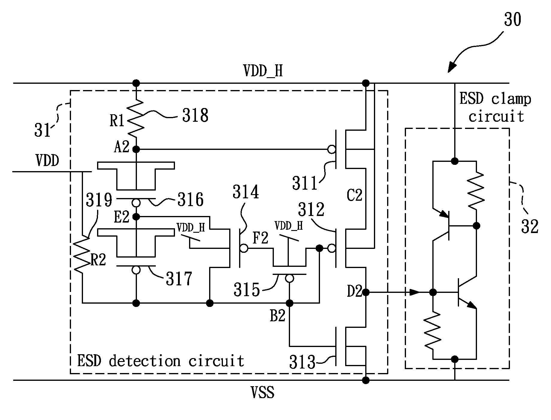
[0018]FIG. 3 is an electrostatic discharge protecting circuit with ultra-low standby leakage current for twice supply voltage tolerance according to the present invention. The electrostatic discharge protecting circuit 30 of the invention includes a substrate driver, a third transistor 313, a start-up circuit, a RC circuit and a second resistor 319. The substrate driver has a first transistor 311 and a second transistor 312 in serious connection, and is connected between a twice supply voltage (VDD_H) and a trigger node D2.

[0019]The third transistor 313 is connected to the trigger node D2. The start-up circuit has a fourth transistor 314 and a fifth transistor 315 with diode-connected, and is connected to the second transistor 312 and the third transistor 313. The RC circuit has a first resistor 318, a sixth transistor 316 and a seventh transistor 317 in serious connection, and is connected to the twice supply voltage (VDD_H) and the third transistor 313. The second resistor 319 is ...


PUM


Abstract

The invention relates to an electrostatic discharge protecting circuit with ultra-low standby leakage current for twice supply voltage tolerance. The electrostatic discharge protecting circuit of the invention includes a substrate driver, a third transistor, a start-up circuit, a RC circuit and a second resistor. The substrate driver has a first transistor and a second transistor in serious connection. The start-up circuit has a fourth transistor and a fifth transistor with diode-connected. The RC circuit has a first resistor, a sixth transistor and a seventh transistor in serious connection. Compared with the prior art, the electrostatic discharge protecting circuit with ultra-low standby leakage current for twice supply voltage tolerance of the invention with advantages of low standby leakage current, high ESD robustness, and no gate-oxide reliability issue is an excellent circuit solution for on-chip ESD protection design for mixed-voltage I/O buffers in nanometer CMOS technologies.

Description

BACKGROUND OF THE INVENTION[0001]1. Field of the Invention[0002]The present invention relates to an electrostatic discharge protecting circuit, more particularly, an electrostatic discharge protecting circuit with ultra-low standby leakage current for twice supply voltage tolerance.[0003]2. Description of the Related Art[0004]With the decrease of the power supply voltage for low power applications, the thickness of the gate oxide has been also scaled down in the nanometer CMOS technologies. The circuit designs quickly migrate to lower VDD voltage level such as 1V in a 65-nm CMOS process to reduce the power consumption. However, some peripheral components or other ICs in a microelectronic system are still operated at the higher voltage levels. With consideration on the whole system integration, the I / O buffers may drive or receive high-voltage signals to communicate with other ICs. Several problems arise in the I / O interface between these ICs, such as the gate-oxide breakdown (referr...

Claims


Application Information

Patent Timeline
Patent Type & Authority Applications(United States)
IPC IPC(8): H02H9/04
CPCH01L27/0262H01L27/0266H01L2924/0002H01L2924/00
Inventor KER, MING-DOUWANG, CHANG-TZUWANG, CHUA-CHIN
Owner NAT SUN YAT SEN UNIV
Why Eureka
Try Eureka